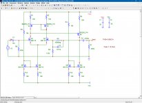
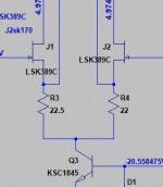
If any one made discrete op-amp which stable at gain 1x, high slew rate (>15V/uS), low distortion (< 0,01% at all audio frequency)?
DC Offset is not importance, input can be BJT.
With gain > 3x it is easy to achieve.
DC Offset is not importance, input can be BJT.
With gain > 3x it is easy to achieve.
Yes, but not for public, it was hard to do, at least for me, but it could be done.BTW, OLG is about 80dB, with higher values I failed to make it stable as a buffer...
Initially I noticed a difficult to null offset,
Unloaded, the response peaked at 250kHz and sinusoids presented distortion in the negative part indicating slew issues.
I reduced IPS current to 4mA (R5 270ohm)
Also reduced VAS current to 9mA (R8 68ohm)
Adjusted output stage idle current to 15mA
Reduced VAS gain by increasing emitter degeneration (R10 57ohm)
And added a capacitor parallel to R10
Now I minimized overshoot and response is flat to 2MHz (unloaded)
Interestingly, the capacitor over R10 must be 330pF when operating at unity gain but it must be higher than 1nF if I use feedback to have gain.
Why is this behaviour possible ?
just measured Slew rate:
1kHz 1Vin
Gain = 1.5X (3.5dB) SR 15V/uS
Gain = 3.0X (9.5dB) SR 16V/uS
Gain = 30X (29.5dB) SR 18V/uS
1kHz 1Vin
Gain = 1.5X (3.5dB) SR 15V/uS
Gain = 3.0X (9.5dB) SR 16V/uS
Gain = 30X (29.5dB) SR 18V/uS
Hi EUVL
Would you care to comment on why do I find the need to have different capacitor bypass on VAS emitter resistor to reduce overshoot when choosing unity gain or seting the DOPA with some gain in non inverting mode ?
Would you care to comment on why do I find the need to have different capacitor bypass on VAS emitter resistor to reduce overshoot when choosing unity gain or seting the DOPA with some gain in non inverting mode ?
The slew rate numbers are suspect. 1 KHz 1V is approx 6 V/mS. 30X gain would make that around 190V/mS or .19v/uS. can you provide more clarity in what you were working out with those slew rate numbers?
The bypass cap on the emitter resistor is changing the loop gain at high frequencies affecting the phase margin. I suspect that circuit is only conditionally stable (from experience with almost the same circuit) so you will have some tuning to deal with at different gains.
The bypass cap on the emitter resistor is changing the loop gain at high frequencies affecting the phase margin. I suspect that circuit is only conditionally stable (from experience with almost the same circuit) so you will have some tuning to deal with at different gains.
In all cases I am using a signal generator set to 1kHz and 1V output
In the scope I read:
Rise time 1kHz (40X Gain) 1.98 uS
BY-AY 36 V
So I believe:
SLEW RATE 18 V/uS
In the scope I read:
Rise time 1kHz (40X Gain) 1.98 uS
BY-AY 36 V
So I believe:
SLEW RATE 18 V/uS
My scope on a 1 KHz sine wave at 1V RMS says 284 uS which makes sense. A sine wave is not a good place to measure rise time. ideally slew rate is calculated from the frequency and amplitude that get around 3% THD. Its an indication that the amp cannot accurately follow the input. However the audio trade uses saturated slew rate because its a bigger number. That's from a square wave where the amps internal circuits are in saturation on a leading edge.
Maybe I read what you posted as a sine wave and you are using a square wave, a simple misunderstanding. In that case you will be looking at saturated slew rate.
Maybe I read what you posted as a sine wave and you are using a square wave, a simple misunderstanding. In that case you will be looking at saturated slew rate.
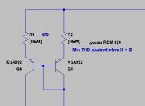
I found that equalizing the currents in the LTP mirror emitter resistors minimizes THD.
That does not mean that the input jfets emitter currents are equal (they are not).
I believed it was the other way around.....
That does not mean that the input jfets emitter currents are equal (they are not).
I believed it was the other way around.....
In my build I use a trimmer over R1 to null output offset..... now I see this is not the ideal as different values over R1 and R2 will surely increase THD.
My experiments indicate that trimming the input fets degeneration resistors can also null output offset but without affecting THD..... but a trimmer there might leave a strong sonic signature...
Can you please indicate the best way to null output offset ?
My experiments indicate that trimming the input fets degeneration resistors can also null output offset but without affecting THD..... but a trimmer there might leave a strong sonic signature...
Can you please indicate the best way to null output offset ?
Attachments
This is what I have used very successfully for offset trim. It limits the current through the pot wiper which is important. The resistor in series with the wiper should be adjusted to the largest that will accomodate worst case offset differential between the two fets.
The pot needs to be a good one. I used vishay foil but those are $$$. Carbon would not be good for this. Possibly a wirewound would be the best reasonable but cermet may be as good.
I have also found that a stable thermal housing and reaching operating temperature is important before attempting to adjust.
I have also found that in some cases the lowest distortion is not at the lowest DC offset of the amplifier. usually this is at the -130 dBC distortion levels or lower.
Attachments

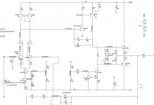
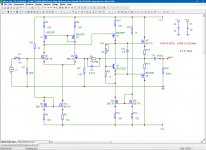
Here the version with low output impedance and output Class-AB stage.> The output would be very high Z so loading will have a big impact on its performance.
> Needs followers to deal with that.
Good advice.
Practically from my experience, the biggest problem will be DC drift.
So the circuitry has to take that into account.
Patrick
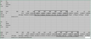
Gain = 60 dB
THD = 0.002 % @300kOhm
THD = 0.005 % @ 32 Ohm.
Fmax = 21 MHz.
Attachments
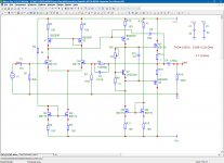
How did you manage to get it stable wo miller comp?Here the version with low output impedance and output Class-AB stage.
Gain = 60 dB
THD = 0.002 % @300kOhm
THD = 0.005 % @ 32 Ohm.
Fmax = 21 MHz.
I did not yet - it is just a concept schematic.How did you manage to get it stable wo miller comp?
I see no problem here. As usual, by just adding C5 of 50pF between output and gate of X4 - solves the problem - the phase reversal of -180 is on 17.5 MHz and the gain there is now near zero. The upper limit reduced to 16 Mhz.
Attachments
Last edited:
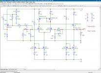
Important note: I strongly beleive that huge part of "transistor sound" (20%) is derived from the fact that transistors ARE SMALLER (smaller controlling area in a device: gate, base are mush smaller than grid in tubes). Skin-effect adds here the distortions and compression.
We can use larger power mosfet AT THE INPUT and in all stages of amplifier. But the input capacitance will be too high. However, it is well-known schematic called bootstrapping to reduce input capacitance.
Some details are here:
BOOTSTRAPPING
I am proposing to use POWER MOSFETS in all stages of amplifiers AND bootstrapping of input stage. For example:
Bootsrapping is provided by M19 power MOSFET.
Attachments
- Home
- Source & Line
- Analog Line Level
- Discrete Opamp Open Design