
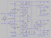
I'm basically done playing in the simulator. Input devices are now LSK489A/LSJ689A but as a pair of pairs because they are dual devices. As R3 is essentially dominant for noise contribution, add another pair of dual input devices to drop R3 in half to drop noise which isn't shabby at 6.6uV. With a clipping at almost rail, that gives a dynamic range of 142.1 dB 😀
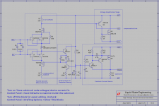
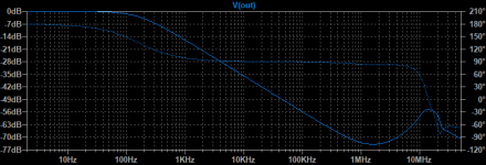
The 17 MHz right-hand zero is still a problem, but I'll find it eventually and I don't think the topology will change, so I'm hitting KiCad next 😎
If anyone can improve this, PLEASE SHARE, thanks.
The 17 MHz right-hand zero is still a problem, but I'll find it eventually and I don't think the topology will change, so I'm hitting KiCad next 😎
If anyone can improve this, PLEASE SHARE, thanks.
Attachments
Be sure to socket the frequency compensation components so you can quickly swap values and find the "cliff of death" where the amp just begins to go unstable. It's guaranteed that you made one or more mistakes in hand calculations and one or more mistakes in simulation, which by Murphy's Law means: your first prototype will break into oscillation, more likely than not.
I like to use (THESE breakaway SIP sockets) on frequency compensation components, but any socket is better than no socket at all.
And, oh by the way, make sure you buy a schmeer of component values for the frequency compensator. Both below, and above, your pre-prototypewild guess estimated values. Ten bucks worth of extra capacitors can save you 3 days of downtime, waiting for a second shipment of parts, not to mention the shipping cost of a second box.
_
I like to use (THESE breakaway SIP sockets) on frequency compensation components, but any socket is better than no socket at all.
And, oh by the way, make sure you buy a schmeer of component values for the frequency compensator. Both below, and above, your pre-prototype
_
All thumbs up! I'm in full agreement, thanks
Attachments
Last edited:
M1, the DN2540 is the ring problem. But I need something with about 2W or more dissipation, same for a replacement of the TP2540 if I'm cascading more jfets for dropping the noise.
It took me a while, but the 15 MHz hump appears to be a problem with the front-end jfets. An inverter gives an output such that difference between the two inputs is zero. They just have a problem at 15 MHz doing that. Why? Dunno.
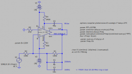
Anyways, here's my final before I hit KiCad to try this out. I switched to using enhancement MOSFETs for both top and bottom of the cascode as part choices are better. The IRFP* parts for M1/2 are just placeholders. The diode spread is now a Vbe multiplier so I can trim the Vds across the jfets. The CCS can be more perfect, but is the closest I can get it for now
Anyways, here's my final before I hit KiCad to try this out. I switched to using enhancement MOSFETs for both top and bottom of the cascode as part choices are better. The IRFP* parts for M1/2 are just placeholders. The diode spread is now a Vbe multiplier so I can trim the Vds across the jfets. The CCS can be more perfect, but is the closest I can get it for now
Attachments
Might want to install 3 more resistors. One in series with each of your 3 compensation capacitors C1, C2, C3. And of course socket all six parts on your first couple of boards.
These resistors introduce pole-zero pairs, which might be very handy for fine tuning the phase response on the lab bench -- you can only do so much in the simulator with device models created by strangers. Adjusting the pole-zero placement will probably help you optimize stability and HF performance. Including that well-loved old favorite of magazine reviews, the dual trace 250 kHz square wave photo. Channel-1 is the perfect 250 kHz square wave applied to your circuit, Channel-2 is the almost-perfect output waveform from your circuit.
And if they're unnecessary, if lab experiments show the optimum resistor value is zero in all three cases, just install jumpers. No PCB revision needed.
- Home
- Amplifiers
- Solid State
- Discrete opamp instability help needed