Hitachi's advancements in amplifier design, particularly through the use of power MOSFETs, have significantly impacted the audio industry. Their balanced voltage amplification stage design, outlined in their application note, transformed the way amplifiers were built, enhancing performance, efficiency, and sound quality.

In the early days, bipolar transistors were the dominant components in amplifier circuits. They were valued for their high gain and efficiency, but as the demand for higher fidelity in audio systems grew, the limitations of bipolar transistors became more apparent. They required higher driving power, were prone to distortion, and exhibited significant phase issues at higher frequencies. Recognizing these challenges, Hitachi was one of the first companies to explore the potential of MOSFETs (Metal-Oxide-Semiconductor Field-Effect Transistors) for high-output amplifier designs.
Hitachi engineers initially worked with small signal MOSFETs used in TV tuners and similar high-frequency applications. Through years of refinement, they adapted this technology to create high-power MOSFETs, which offered significant improvements over traditional bipolar transistors. This led to the development of amplifier circuits that took full advantage of MOSFET characteristics, particularly through the balanced voltage amplification stage.
According to the application note, power MOSFETs offer several distinct advantages over bipolar transistors, making them ideal for high-performance audio amplifiers. Power MOSFETs are voltage-controlled devices, which means they require significantly less driving power compared to bipolar transistors. Unlike bipolar transistors, MOSFETs are free from current concentration, making them far more resistant to damage from electrical stress or thermal runaway. The absence of carrier storage effect in MOSFETs enables a high switching speed and excellent frequency response.
While power MOSFETs brought clear advantages, their inherent distortion (approximately 20 dB higher than bipolar transistors) required Hitachi engineers to rethink the design of the voltage amplification stage. To mitigate this distortion, they developed a balanced voltage amplification stage, which allowed them to increase the open-loop gain and apply larger amounts of negative feedback—key to reducing distortion without compromising bandwidth.

The balanced voltage amplification stage works by taking signals from both the inverting and non-inverting outputs of the long tail pair input stage, a critical design decision that maximizes the amplifier’s ability to reject common-mode noise and increase overall gain. By amplifying both signal paths symmetrically, Hitachi’s engineers were able to apply larger amounts of negative feedback over a wide frequency range, effectively reducing distortion.
In bipolar transistor designs, a Darlington connection is often used to increase bandwidth. However, this two-stage emitter follower configuration introduces significant phase distortion, which complicates the application of negative feedback. To compensate for this, phase compensation circuits are required, which can further degrade performance by sacrificing gain and limiting the overall frequency response.
Power MOSFETs, on the other hand, offer a significant advantage. With a single MOSFET source follower, large amounts of negative feedback can be applied over a broad frequency range without the same phase issues. This allows for greater stability and lower distortion, particularly at high frequencies. Furthermore, the driver stage of a MOSFET does not require a conventional class B driver, which reduces the number of components and simplifies the amplifier design.
From the application note on design of voltage amplifier stage:
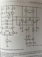
"A power MOS FET can be used with a low driving power. Fundamentally, only the power for charging and discharging the gate-to-source capacitance is needed to the output stage, so that no class B driver stage is required. The driving power varies with input frequency. At 100 W output and 10 kHz frequency it would be about 10 mW. Therefore, an output stage power MOS FET can be driven directly from a class A predriver (voltage amplifier stage) used in a bipolar transistor amplifier. By eliminating the class B driver, the number of components can be reduced, and impairing the amplifier's performance caused by the driver itself can be avoided. Further, the number of poles for transfer function (open loop gain vs. frequency characteristics) decrease, and the stagger can easily be increased. Consequently, the stability against oscillation is improved. Transistors for the voltage amplifier stage are required to have a high voltage durability, low Cob and high fT. Here the 2SD756A/2SB716A developed especially for power MOS FETs are used. With the NPN differential amplifier and PNP constant current load, high gain and low distortion characteristics were obtained. The class A stage bias current is set as 10 mA. When bias current is lacking, sufficient power to drive a power MOS FET at high frequency cannot be supplied, and distortion would worsen. The drain current temperature coefficient of a power MOS FET undergoes a reversal of polarity at around ID = 100 mA and temperature compensation in the large current region will be unnecessary. Hence, the bias circuit for a power MOS FET is vastly simplified because only one semifixed resistor (1 kOhm) for setting idling current will suffice. For the input stage, a stable differential amplifier circuit was formed by using the high-voltage, low-noise transistor 2SA872, which is known for its high performance in improving the S/N ratio. Bias current is set as 0.5 mA."
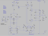
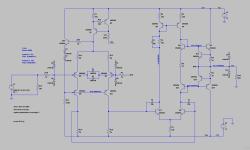
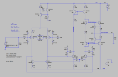
Inspired by Hitachi’s innovations, I have decided to create an op-amp design based on the differential voltage amplification stage. This design leverages the balanced approach to drive the output stage of the op-amp, optimized for small signal processing. Since typical op-amp loads are as low as 600 ohms, compared to the 4-ohm loads found in power amplifiers, the current-driving requirements are much lower.
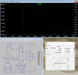
Opamp specs:
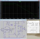
THD (G=+1, 600R, Vin=1.41Vrms, 1kHz): 0.000007% or -143dB
THD (G=+1, 600R, Vin=8.5Vrms, 1kHz): 0.000054% or -125dB
BW (G=1): 10MHz
Noise: 1.95 nV/Hz1/2
Voffset: 0.02mA
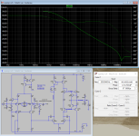
AOL (100Hz): 110dB
AOL (20kHz): 80dB
Attached you can find Hitachi app note and opamp design in LTSpice simulation.
In the early days, bipolar transistors were the dominant components in amplifier circuits. They were valued for their high gain and efficiency, but as the demand for higher fidelity in audio systems grew, the limitations of bipolar transistors became more apparent. They required higher driving power, were prone to distortion, and exhibited significant phase issues at higher frequencies. Recognizing these challenges, Hitachi was one of the first companies to explore the potential of MOSFETs (Metal-Oxide-Semiconductor Field-Effect Transistors) for high-output amplifier designs.
Hitachi engineers initially worked with small signal MOSFETs used in TV tuners and similar high-frequency applications. Through years of refinement, they adapted this technology to create high-power MOSFETs, which offered significant improvements over traditional bipolar transistors. This led to the development of amplifier circuits that took full advantage of MOSFET characteristics, particularly through the balanced voltage amplification stage.
According to the application note, power MOSFETs offer several distinct advantages over bipolar transistors, making them ideal for high-performance audio amplifiers. Power MOSFETs are voltage-controlled devices, which means they require significantly less driving power compared to bipolar transistors. Unlike bipolar transistors, MOSFETs are free from current concentration, making them far more resistant to damage from electrical stress or thermal runaway. The absence of carrier storage effect in MOSFETs enables a high switching speed and excellent frequency response.
While power MOSFETs brought clear advantages, their inherent distortion (approximately 20 dB higher than bipolar transistors) required Hitachi engineers to rethink the design of the voltage amplification stage. To mitigate this distortion, they developed a balanced voltage amplification stage, which allowed them to increase the open-loop gain and apply larger amounts of negative feedback—key to reducing distortion without compromising bandwidth.
The balanced voltage amplification stage works by taking signals from both the inverting and non-inverting outputs of the long tail pair input stage, a critical design decision that maximizes the amplifier’s ability to reject common-mode noise and increase overall gain. By amplifying both signal paths symmetrically, Hitachi’s engineers were able to apply larger amounts of negative feedback over a wide frequency range, effectively reducing distortion.
In bipolar transistor designs, a Darlington connection is often used to increase bandwidth. However, this two-stage emitter follower configuration introduces significant phase distortion, which complicates the application of negative feedback. To compensate for this, phase compensation circuits are required, which can further degrade performance by sacrificing gain and limiting the overall frequency response.
Power MOSFETs, on the other hand, offer a significant advantage. With a single MOSFET source follower, large amounts of negative feedback can be applied over a broad frequency range without the same phase issues. This allows for greater stability and lower distortion, particularly at high frequencies. Furthermore, the driver stage of a MOSFET does not require a conventional class B driver, which reduces the number of components and simplifies the amplifier design.
From the application note on design of voltage amplifier stage:
"A power MOS FET can be used with a low driving power. Fundamentally, only the power for charging and discharging the gate-to-source capacitance is needed to the output stage, so that no class B driver stage is required. The driving power varies with input frequency. At 100 W output and 10 kHz frequency it would be about 10 mW. Therefore, an output stage power MOS FET can be driven directly from a class A predriver (voltage amplifier stage) used in a bipolar transistor amplifier. By eliminating the class B driver, the number of components can be reduced, and impairing the amplifier's performance caused by the driver itself can be avoided. Further, the number of poles for transfer function (open loop gain vs. frequency characteristics) decrease, and the stagger can easily be increased. Consequently, the stability against oscillation is improved. Transistors for the voltage amplifier stage are required to have a high voltage durability, low Cob and high fT. Here the 2SD756A/2SB716A developed especially for power MOS FETs are used. With the NPN differential amplifier and PNP constant current load, high gain and low distortion characteristics were obtained. The class A stage bias current is set as 10 mA. When bias current is lacking, sufficient power to drive a power MOS FET at high frequency cannot be supplied, and distortion would worsen. The drain current temperature coefficient of a power MOS FET undergoes a reversal of polarity at around ID = 100 mA and temperature compensation in the large current region will be unnecessary. Hence, the bias circuit for a power MOS FET is vastly simplified because only one semifixed resistor (1 kOhm) for setting idling current will suffice. For the input stage, a stable differential amplifier circuit was formed by using the high-voltage, low-noise transistor 2SA872, which is known for its high performance in improving the S/N ratio. Bias current is set as 0.5 mA."
Inspired by Hitachi’s innovations, I have decided to create an op-amp design based on the differential voltage amplification stage. This design leverages the balanced approach to drive the output stage of the op-amp, optimized for small signal processing. Since typical op-amp loads are as low as 600 ohms, compared to the 4-ohm loads found in power amplifiers, the current-driving requirements are much lower.
Opamp specs:
THD (G=+1, 600R, Vin=1.41Vrms, 1kHz): 0.000007% or -143dB
THD (G=+1, 600R, Vin=8.5Vrms, 1kHz): 0.000054% or -125dB
BW (G=1): 10MHz
Noise: 1.95 nV/Hz1/2
Voffset: 0.02mA
AOL (100Hz): 110dB
AOL (20kHz): 80dB
Attached you can find Hitachi app note and opamp design in LTSpice simulation.
Attachments
Last edited:

Long ago I made a protoype amp which used an input diff pair and vas similar to that used in your schematic. Whilst it worked fine and the distortion was low, it was higher than in the original design with resistors, rather than current mirrors, loading the input diff pair. With real world parts ( not sim ) the current mirrors on the input diff pair and vas "fight" against each other and unbalance the circuit leading to higher distortion. I have tried on and off over the years to try and improve the Hitachi design, without much success. The only thing I have found to be worthwhile is a constant current source, rather than a resistor, in the tail of the input diff pair. The usual two transistor circuit works well, but you can save a transistor, as well as making the vas fully differential, by trying the old JLH tick of using a jfet, driven from the vas, to set the input diff pair current. You don't then need R6. Cascoding might be necessary if you don't have access to the obsolete japanese low noise, high beta, high voltage transistors. Using super beta transistors like the 2SC3071 for the vas didn't seem to make a worthwhile improvement. Darlington pairs for the vas only make a measureable improvement in performance if all four transistors are extremely closely matched, otherwise they make it worse. All diff pairs and mirrors should be closely matched if possible. I haven't experimented much with the output stage so maybe something like Lazy Cat's BIGBT might make a difference. Personally I think that the Hitachi circuit is one of the all time greats. Opinions may differ.
To preserve symmetry, you could put a common-mode loop rather than a current mirror below the first stage. Without the cascodes Q5 and Q11, you would only have to connect the base rail of Q12 and Q20 to the emitters of Q17 and Q6, disconnect it from Q12's collector. You don't even have to resize the resistors.

Last edited:
I would also add a stack of four series-connected diodes between the base rail of Q18 and Q19 and the negative supply.
I like your antiparallel diodes, by the way. Almost no one protects their transistors against base-emitter avalanche breakdown, nice to see that you do.
I forgot to connect the base of Q6. Corrected:

I like your antiparallel diodes, by the way. Almost no one protects their transistors against base-emitter avalanche breakdown, nice to see that you do.
I forgot to connect the base of Q6. Corrected:
Last edited:
Have you tried using degenerative resistors for VAS emitters? I tried it in sim and 10R at each VAS transistor seems to be working fine. You would need to change rail resistor to 47R.I have tried on and off over the years to try and improve the Hitachi design, without much success.
Bob Cordell suggests to put a buffer in front of each VAS - maybe that is also a way to fix it.
Attachments
Yes tried that and as you say it works fine. The other thing I have tried that also works well is to set the tail current of the input diff pair with a jfet tied to the non driven transistor collector of the vas. This sets the diff pair tail current to Idss of the jfet and the collector voltage of the non driven vas transistor to 0V ( no resistor or cascode transistor required ). The other things that I intend to try are a common mode control loop instead of resistors loading the input differential pair and a full Wilson current mirror loading the vas. These mods should improve the symmetry and lead to a reduction in thd. Probably won't sound any better but I'll feel better about it. The jfet "trick" was suggested decades ago by John Lindsley Hood, and the common mode loop by MarclevdG (see above), as well as others, on this forum. I'll post a hand drawn schematic tomorrow to illustrate what I mean.

Your drawing reminded me of ISP with bootstrapped cascode.
Common mode distortion special lol.
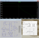
OLG 20khz is at impressive 68db!
Common mode distortion special lol.
OLG 20khz is at impressive 68db!
Attachments
Last edited:
Added two emitter degeneration resistors 33R each to VAS and it worked!
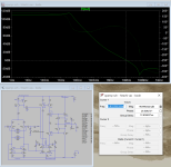
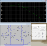
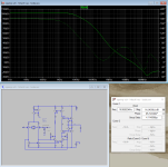
After adding two pole compensation the slew rate is at 45V/uS!
OLG is at 102dB at 100Hz and 91dB !!! at 20kHz.
After adding two pole compensation the slew rate is at 45V/uS!
OLG is at 102dB at 100Hz and 91dB !!! at 20kHz.
Attachments


- Home
- Source & Line
- Analog Line Level
- Discrete OPAMP based on balanced VAS from HITACHI app note with Two Pole Compensation OLG 80dB at 20kHz