After some discussion about how best to attenuate volume between a DAC and a power amp, I have ordered a simple FET buffer PCB from SKA Audio and have decided to post a build diary.
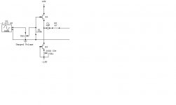
The schematic is attached below. Note that the pcb is just a prototype so does not appear to be commercially available yet.
Here's a bill of materials (in case anyone is also interested in doing a build):
For the pcb:
1 x 10K Stereo Potentiomenter
2 x 47R 1/4W Resistor
2 x 100K 1/4W Resistor
2 x 1uF 50V capacitors (I'm using 0.22uF polypropylene caps)
2 X 100R trimpot
Remaining items:
Chassis
Regulated DC power supply + transformer
IEC socket + fuse socket
RCA jacks (input and output)
2 x 47R 1/4w Resistor (for placing from the output of the pcb to the RCA outputs)
Hookup wire & Solder
Knob for volume pot
I'll post some pictures and further comments as it progresses, but any thoughts on the design, etc, would be great!
Attachments
Last edited:
.
.
1 x 10K Stereo Potentiomenter
.
.
. . . any thoughts on the design, etc, would be great!
Keep in mind, if your source has an output impedance of 10k ohms (like my SACD player), then with a 10k potentiometer, you have - 6 dB attenuation at full volume. (I choose a 10k ohm attenuator, as you and don't worry about the extra - 6 dB.)
.
Thanks John – what is the calculation for working out the dB range? My cd player has an output impedance of 22 Ohms and the power amp an input impedance of 100K ohms.
Keep in mind, if your source has an output impedance of 10k ohms (like my SACD player)...
Your SACD player has an output impedance of 10k ohms?
Man, get that thing into the shop and have it fixed, or get a rescue inhaler for whatever asthmatic tube output stage it's running. 😀
se
Thanks John – what is the calculation for working out the dB range? My cd player has an output impedance of 22 Ohms and the power amp an input impedance of 100K ohms.
If your CD Player has an output impedance of 22 ohms and you're driving it into a 10k attenuator, then at full volume, you'll have a signal attenuation of about 0.02dB. Nothing to worry about.
se
It's a Sony player. I can't find the spec. sheet online, but I measured it too--it's 10k. It's probably a series resistor? I should change that to 100 ohms, if I can. Thanks, Steve!
.
.
I measured it too--it's 10k.
And *how* did you measure this figure? You can't just use the Ohms function of your DMM for this.
Samuel
And *how* did you measure this figure? You can't just use the Ohms function of your DMM for this.
Samuel
Well . . . measured 1 Vrms (@ 1khz) out unloaded and 0.5 Vrms loaded with a 10k ohm resistor. (Again, the hardcopy spec sheet indicates 10 k ohm output too.)
.
What JFET you plan to use?
Maybe 2SK170BL
2SK170GR has got lower current, but we prefer high current
http://www.ska-audio.com/Forum/YaBB.pl?num=1244063607/0
Greg says this:
Maybe 2SK170BL
2SK170GR has got lower current, but we prefer high current
http://www.ska-audio.com/Forum/YaBB.pl?num=1244063607/0
Greg says this:
Re: A Simple FET Buffer
Reply #2 - Jun 5th, 2009, 8:33am
Hi Mugsy,
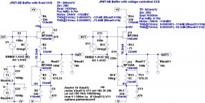
You can use the 2SK170 GR,BL, or V..... or ungraded, I simmed it with the SMD BF862 but can input any 2SK170 variant, or even the BF244B.
The 61R resistor was chosen to set the standing Class A current to 5mA, that will vary with the device. The DC null trimpot is VR1 and a 100R should give enough range for a null.
A 25K Alps pot can simply connect conventionally at the input where V2 (the sim test signal source) is shown, input coming from the wiper.
Greg
Last edited:
I'm not sure about the technical advantages of this transistor - but I'll use:
2SK117 N channel Toshiba low noise FET (4 pcs)
2SK117 N channel Toshiba low noise FET (4 pcs)
Hi,
it can´t work...there are no JFETs listed in the BOM 😀
As JFETs You might consider the Philips/NXP types BF246A or 247A in TO92-casing. They are cheap, easy to source and well suited for this application (high IDSS values).
Add a source resistor between Q1´s source and output! With 75Ohms source resistor the BF24A run on app. 18mA bias current.
The CCS-JFET´s source resistor could be a 75Ohms resistor or a 82Ohm paralleled with a 2k-pot to trim for lowest voltage-offset.
Power supply lines should be reduced to 10V or less to reduce heat power in the JFETs.
Output impedance is app 100Ohms, so You might omit with R3.
You might even omit with C1 if the source is DC-free. Or You may change the position and value of C1 by changing R1 to 2M2 and placing a smaller valued C1 (100nF-220nF) between VR3 and R1. Q1 and Q3 then need to be closely matched and thermally coupled though.
The Buffer can supply a maximum current equal to the bias current into the load. If You need more current You can either reduce the source resistor values (beware power ratings!) or You change from a fixed CCS to a voltage steered CCS. As You can see from the THD-simulation it will be advantageous to use the voltage controlled CCS with low Load-impedances.
Add a resistor between positive supply and Drain of J1 (270-330Ohms). Add a 100nF-220nF cap from J1´s Drain to J2´s Gate. Connect a 1M-2M2 resistor from Q3´s Gate to the negative supply. Add a second resistor of 270-330Ohms between negative supply and J2´s source-R. The result is the circuit ton the left.
jauu
Calvin
Attachments
Last edited:
combining the post10 setting up description from SKA and the schematic of post1, I can see that the buffer jFET is being run at Idss.
That makes it the same philosophy as the B1. Except that the B1 uses a pair of selected jFETs that will help compensate for output offset with temperature changes.
I would rather use a B1 or change the schematic to that shown by Feucht, in Buffer amplifier design.
Post12, the left hand diagram with fixed CCS is Feucht.
Last edited:
To stay close to Greg's SKA circuit
this is my suggestion.
Some notes:
1. R2 and C1 is a lowpass filter rolling off at 1.5 MHz
Without, my sim shows upper -3dB at 900 MHz = Radio frequencies.
2. I use JFETs with IDSS = 8mA
Run them at 6 mA
3. R1, 15 Ohm, in FET source gives 0.0 Volt at output.
So output capacitor is not needed.
I ran SPICE with capacitor and without capacitor.
Like in my schematic with 15 Ohm resistor without capacitor
gave a little tiny bit better performance.
Regards Lineup
Attachments
Hi Lineup,
Are your references to the SKA schematic, or your schematic?
Ideally, I'd like to build it without capacitors, but it might ultimately be easier just to use them.
I forgot to mention some comments Greg has given me in relation to the buffer schematic:
1. The FETS should be measured for Idss and preferably with one significantly higher for the CCS (Q3). Preferred types are GR 2SK170's or 2SK117's
2. The output coupling cap is only needed if cannot get stable DC at 0mV within acceptable error tolerance, otherwise link out.
3. Supplies of +/-10V will reduce drift due to warmup.
Cheers,
LE
Idss is the current passing when 10Vds and 0Vgs are applied to the jFET.
0Vgs is saying that the input voltage at the gate is equal to the output voltage at the source.
If the current is ><Idss then Vgs cannot be zero, i.e. there must be an output offset.
The extra source resistor in the Feucht buffer adds an extra voltage drop.
This resistor can be adjusted so that when output is taken from the bottom of this resistor the output offset can be zero even though the jFET is passing a current><Idss.
Go and read Feucht.
- Status
- Not open for further replies.
- Home
- Amplifiers
- Solid State
- Discrete Fet Buffer - Build Diary