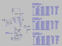
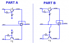
New idea = 1 mmbf4391 cascode for the two 2sk389bl JFETs, but reducing Vds over this cascode by implementing a second cascode to reduce Pdiss ... cascoding the cascode.
Will try to draw this tomorrow!
Will try to draw this tomorrow!
Less is more
I've reduced PSU voltages to have an allowable power dissipation into the SOT-23 Jfet.
I've increased the bias currents to 10mA into the 2Sk389 Jfet's (have plenty of them with around Idss of +-11mA.
Distorsion is unbelievable low, simulated at 0.3v and 2Vrms ?? Yeah, simulation, I know, but still.
Will start collecting some of the components I dont have laying around and will make a prototype.
Yet to find an easy way to adjust/trim DC-offset.
Attachments
Last edited:
New idea
Tracking cascode with TO-220 mosfets and higher Idss grade jfets.
Don't have higher Idss Jfet's available. Other question is, where to still find them nowadays.
I've noticed that a tracking cascode has quite some impact on the THD while this loads the output. With an additional stage (as in the Calvin Buffer) the tracking cascode has a much bigger positive impact.
I've noticed that a tracking cascode has quite some impact on the THD while this loads the output. With an additional stage (as in the Calvin Buffer) the tracking cascode has a much bigger positive impact.
Hi,
I've been using the 389(suffix B)/3941 JFET-combo for many years.
Typically the 389 then run on around 4V Vds, which keeps them safely in their linear range.
After my experience the LSK389 seem to be quite sensitive against LatchUp.
Be aware when running them on loads of bias current, especially with large valued gate resistors. Costed me quite a couple of buffers.
This was one of the reasons to develop the Calvin buffer.
I could have switched to depletion mode MOSFETs like the BSSxxx or BSPxxx from Infineon for increased current capabilities, but I liked the 389s otherwise superior performance.
Adding the bipolar booster in Sziklai fashion not only allows for a far greater possible current range than with depletion mode FETs, but also reduces the current swing in the 389, thereby reducing THD of the whole circuit at higher load currents.
Regarding the offset issue ... it won't be all to easy to keep it low and constant, as the temperature drift of the buffer and the ccs probabely don't match/track.
Using the buffer topology also as the current source allows trimming of the static offset and -if the master JFETs are matched and thermally coupled- the tracking of the temperature related offset drift.
On my website I show a dc-servo design for the Calvin buffer that directly controls the current of the ccs. It can be implemented with Your bioolar ccs also.
jauu
Calvin
Don't have higher Idss Jfet's available. Other question is, where to still find them nowadays.
They can be just paralleled.
Note, you need not only higher Idss, this could be easily picked from something like PN4391 or J108, but simultaneously high Idss and transconductance.
Mosfet second stage keeps JFET dissipation lower while dramatically drops output resistance. So if you can find Crystallonics CP650 JFET you can easily build very potent headamp.
Just add real load to the output and impact of higher Idss and trasconductance will be much visible.I've noticed that a tracking cascode has quite some impact on the THD while this loads the output.
Attachments
I've reduced PSU voltages to have an allowable power dissipation into the SOT-23 Jfet.
I've increased the bias currents to 10mA into the 2Sk389 Jfet's (have plenty of them with around Idss of +-11mA.
Distorsion is unbelievable low, simulated at 0.3v and 2Vrms ?? Yeah, simulation, I know, but still.
Will start collecting some of the components I dont have laying around and will make a prototype.
Yet to find an easy way to adjust/trim DC-offset.
Hey thx for your project, I am looking forward to see if your circuit will sound great ( I am looking for a upgrade to PGA2310)
Maybe you will sell pcb some day?
Maybe with integrated low noise regulator?
Best regards
Hi,
After my experience the LSK389 seem to be quite sensitive against LatchUp.
Be aware when running them on loads of bias current, especially with large valued gate resistors. Costed me quite a couple of buffers.
jauu
Calvin
Can you please explain further? Do you mean the gate stopper or shunt resistor to gnd? I can't understand why this can do any harm, but I'm definetely not the expert! Is this specific for the LSK devices or did you have the same experience with the Toshiba's?
regards
Hi,
the gate leakage current flows -as small as it is at the beginning- through the shunt-to-ground, changing the Vgs of the JFET.
If the shunt is high valued and the leakage grows due to heating up of the JFET its drain current rises, resulting in more heat, resulting in more leakage .... till latchup.
Some datasheets show the leakage over temperature over Vds.
Never tried it with Toshibas 389s, just the LSKs.
But the mechanism itself is inherent to all JFETs.
IIre there's a chapter in Horowitz-Hill describing the mechanism.
jauu
Calvin
Thank Calvin,
Was not aware of this mechanism, now that you tell me, it certainly makes sense.
Gate leakage is dependant on temperature, Vds and Id. Were Vds plays the most important role if I go through the paper below (1041 pages!).
With the 4391 as cascode Jfet, Vds will be around 4V, which results in a dissipation of only 40mW (Id = 10mA).
This should not give any problems in my experience. I'm running 389bl's for years at around 80mW, with a gate shunt resistor of 47k.
https://www.pearl-hifi.com/06_Lit_A...pers/Horowitz-Hill/The_Art_of_Electronics.pdf
Hi, Kimschips
Well, I have never done special things regaring ESD.
I have a Weller WS81 solder station, the manual mentiones that is ESD-safe. Whatever this means in practice I don't know.
I have a wooden workbench, isolated from ground with plastic(isch) feet.
Well, I have never done special things regaring ESD.
I have a Weller WS81 solder station, the manual mentiones that is ESD-safe. Whatever this means in practice I don't know.
I have a wooden workbench, isolated from ground with plastic(isch) feet.
Hi, Kimschips
Well, I have never done special things regaring ESD.
I have a Weller WS81 solder station, the manual mentiones that is ESD-safe. Whatever this means in practice I don't know.
I have a wooden workbench, isolated from ground with plastic(isch) feet.
Yes yes seems fine😊
Happy building, I am looking forward to follow this thread.
Best regards
start building - issues offcourse
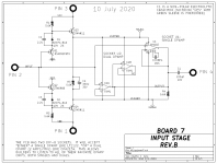
What have I build:
1: CRCRC power supply
2: Jung didden superreg (remote sensing used in combination with the 10R +10n RC combination as advised and LOW ESR output cap Nichicon fine gold)
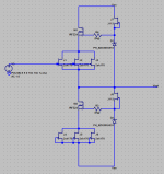
3: buffer as per schematic attached.
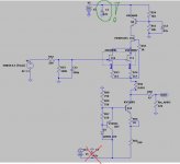
After connection of all PCB's, there was very high frequency oscillation (+-200mHz). After playing wiht the elektrolytic caps on the buffer PCB this is what I noticed.
The 47µF cap at +rail must be connected the 47µF cap at the -rail must NOT be connected. (see red and green marked in the schematic).
I don't undertand the reason why it does not work with both 47µF caps connected.
BTW: when I have oscillation on the output of the buffer I also have it on the output of the Jung Didden superreg.
What have I build:
1: CRCRC power supply
2: Jung didden superreg (remote sensing used in combination with the 10R +10n RC combination as advised and LOW ESR output cap Nichicon fine gold)
3: buffer as per schematic attached.
After connection of all PCB's, there was very high frequency oscillation (+-200mHz). After playing wiht the elektrolytic caps on the buffer PCB this is what I noticed.
The 47µF cap at +rail must be connected the 47µF cap at the -rail must NOT be connected. (see red and green marked in the schematic).
I don't undertand the reason why it does not work with both 47µF caps connected.
BTW: when I have oscillation on the output of the buffer I also have it on the output of the Jung Didden superreg.
Attachments

Just released: M2x daughter card "IPS7". It bootstraps the power supply rails. Also notice resistor "R4". Because the supply rails are bootstrapped, the incremental ("small signal") voltage across R4 is zero. Thus R4 operates as a constant current source, drawing a constant DC current from the output stage, which reduces crossover distortion and increases the gm of the output devices.
Maybe some of these ideas could possibly apply to this circuit requirement, too?
_
Maybe some of these ideas could possibly apply to this circuit requirement, too?
_
Attachments
What have I build:
1: CRCRC power supply
2: Jung didden superreg (remote sensing used in combination with the 10R +10n RC combination as advised and LOW ESR output cap Nichicon fine gold)
3: buffer as per schematic attached.
After connection of all PCB's, there was very high frequency oscillation (+-200mHz). After playing wiht the elektrolytic caps on the buffer PCB this is what I noticed.
The 47µF cap at +rail must be connected the 47µF cap at the -rail must NOT be connected. (see red and green marked in the schematic).
I don't undertand the reason why it does not work with both 47µF caps connected.
BTW: when I have oscillation on the output of the buffer I also have it on the output of the Jung Didden superreg.
I can't see the whole reg board. Anyway, this is a home-brew board, right?
Jan
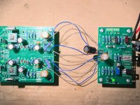
Dear Jan,
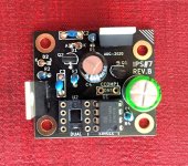
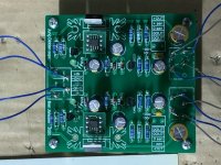
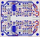
Yes it is home brew, this in order to use some personal standards like connectors and PCB details. Also the distance between the mounting holes is adapted to other PCB's to make them easily stackable.
Enclosed, you can find a full picture of the PCB and the layout. Remark: connectors are not assembled and components are mounted with about 10mm from the PCB as this is only a trial PCB. I would like to reuse most of the components.
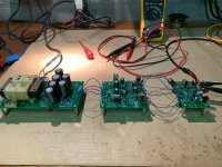
When resistive loading the superreg, I don't see any sort of instability on the Rigol scope (bought from you about a year ago). Also adding extra capacity to the supperreg output cap (LOW-ESR), even a panasonic FC, doesn't lead to instability.
Yes it is home brew, this in order to use some personal standards like connectors and PCB details. Also the distance between the mounting holes is adapted to other PCB's to make them easily stackable.
Enclosed, you can find a full picture of the PCB and the layout. Remark: connectors are not assembled and components are mounted with about 10mm from the PCB as this is only a trial PCB. I would like to reuse most of the components.
When resistive loading the superreg, I don't see any sort of instability on the Rigol scope (bought from you about a year ago). Also adding extra capacity to the supperreg output cap (LOW-ESR), even a panasonic FC, doesn't lead to instability.
Attachments
Why is a buffer + SR needed here?
The buffer circuit below has an Rin of ~100k, and it drives 47K? Is any buffer needed at all?
https://www.diyaudio.com/forums/analog-line-level/350773-discrete-buffers-4.html#post6319660
Even if it is needed, using a SR to feed it seems overkill, unless there are other heavier loads.
Why is remote sensing needed for a ckt only about 10" removed? This could be part of the instability.
Walt Jung
Dear Mr. Jung,
In front of this buffer, a Muses 72320 volume control chip will be used. A buffer after this IC is highly recommended. (output resistance is changing depending on volume setting and datasheet of the 72320 recommends minimum 100k load)
I don't know if this is overkill, after reading the Lineair Audio article from John Walton about the listening tests, I was certain that I needed this superreg.
And if I wouldn't have done it, I would keep on questioning whether it would make things better.
When connecting the sense points directly with the output on the SR PCB, oscillation is identical.
Kind regards
My point was that the difference with/without the buffer is 100k vs. 47k.
Yes, the rout variation of a level control can cause problems if you have appreciable cap loading. But, I’d bet that the 389s could be higher cin than your power amp. But, you do have them bootstrapped, which is very good.
A well constructed SR ckt should NOT oscillate with a wide range of medium (0.1 - 1 ohm) esr electrolytics. I know this to be true, since I recently ran many tests over a range of 10 - 120 uF and the reg loaded with 60mA dc, plus a pulsed dynamic load of 100mA. No ringing, no overshoot, no instability. Even with an Oscon across Vout.
Film caps with very high Q will definitely make it oscillate, and should be avoided. Looking at your circuit, you have 47uF on each rail. What type? You likely don’t even need any cap bypass there, since the SR has a ~100uF cap a few inches away, and the zout is a milliohm or so. Best bypass you might find, in fact. I’d try pulling out the 47uFs and see what that does.
Walt Jung
Last edited:
- Home
- Source & Line
- Analog Line Level
- Discrete buffers