It all started when I started researching about Current Feedback Amplifier
I found this
http://hifisonix.com/wordpress/wp-content/uploads/2017/10/CFA-Front-End.pdf
Before trying to make a full blown Class AB 100W CFA amplifier with Quasi Complimentary FET output.
I made my mind to try to make a Line Level Preamp with CFA input stage with Class A Operation.
Main purpose for me is to learn solid state Amplifier design, I am bored with OP-AMP at this point of time.
Design goals[More like Wish list]:-
*10Vpp Swing without Clipping with Dual 18V supply.
*Complete Class A Operation
*Zero Global Negative Feedback [Local Compensation is necessary]
*Harmonic Profile Shall be Dominated by H2
*H3 shall be close to H2 to add necessary psycho acoustic feel of detail.
*Anything higher than H4 shall be below -120db [As H5 and Higher are responsible for listening fatigue]
*Higher order than H2 shall descent monotonically and H2 increases with increase in Frequency
*Close to 200V/us Slew rate
*Higher than 400Khz bandwidth
Use Cases:
*Line Pre Amplifier
*Headphone Amplifier for Inefficient Planer Headphone

I hope all of you will help me in my journey to make some Solid state amp
🙂
I found this
http://hifisonix.com/wordpress/wp-content/uploads/2017/10/CFA-Front-End.pdf
Before trying to make a full blown Class AB 100W CFA amplifier with Quasi Complimentary FET output.
I made my mind to try to make a Line Level Preamp with CFA input stage with Class A Operation.
Main purpose for me is to learn solid state Amplifier design, I am bored with OP-AMP at this point of time.
Design goals[More like Wish list]:-
*10Vpp Swing without Clipping with Dual 18V supply.
*Complete Class A Operation
*Zero Global Negative Feedback [Local Compensation is necessary]
*Harmonic Profile Shall be Dominated by H2
*H3 shall be close to H2 to add necessary psycho acoustic feel of detail.
*Anything higher than H4 shall be below -120db [As H5 and Higher are responsible for listening fatigue]
*Higher order than H2 shall descent monotonically and H2 increases with increase in Frequency
*Close to 200V/us Slew rate
*Higher than 400Khz bandwidth
Use Cases:
*Line Pre Amplifier
*Headphone Amplifier for Inefficient Planer Headphone
I hope all of you will help me in my journey to make some Solid state amp
🙂
Attachments
For 10Vpp you only need +/-8V supplies. Did you mean 10V peak or 20V swing? Theoretically you can get upto about 11Vrms from +/-18V which is 15.5V peak.*10Vpp Swing without Clipping with Dual 18V supply.
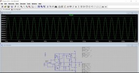
Evidently, its looking very strange at the moment, like Q4's base being hardwired to the rail, and using 2 NPN's won't work in a class B circuit like the input stage, complementary devices are needed.Above Image is just concept.
I made bit changes , Output seems to be negative swing bit weird , added all model.
I dont know how to fix it.
Performance doesn't look good either , Similar VFA circuit will give result 4 decimal point of THD.
I attached everything below I am doing something wrong for sure
Hi Mark , Thanks for looking into it , thats a mistake i made , that one shall be PNP.
https://www.diyaudio.com/forums/members/mark-tillotson.html
Attachments

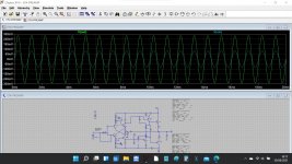
There are a whole bunch of errors in that circuit but even when corrected its still unbalanced.
Q7, Q2 Q4 and Q6 are wrong.
D1 looks suspect. How does that work?
Is it meant to use a complementary output pair? Why is the base of Q6 connected to emitter of Q3?
What does R11 do?
Q7, Q2 Q4 and Q6 are wrong.
D1 looks suspect. How does that work?
Is it meant to use a complementary output pair? Why is the base of Q6 connected to emitter of Q3?
What does R11 do?
Attachments
Hi Mooly,
Q3 and Q4 are VAS and Q5 Q6 are push pull output buffer.
This is nothing new , it is same blameless topology invented by Douglas Self.
I don't know what R11 does , it was their on CFA pdf i found.
D1 prevents short which may occur due to Resistor above it. ( It suppose to be 1N4148)
Thanks for all help.
R11 as drawn is simply an additional load the output has to drive.
D1 seems to be severely limiting the ability of Q3 to turn on. The 0.6v drop of the diode is clamping the base to the negative rail.
If Q6 base is connected to Q3 emitter then Q6 is just turned fully on via the 56 ohm. There is no obvious means of current control and the current is consequently very high, over 1 amp.
Hi Mooly,
Thanks a lot for your time to fix the amp.
I think i need to fix the output stage to reduce power draw.
Thanks a lot for your time to fix the amp.
I think i need to fix the output stage to reduce power draw.
- Home
- Amplifiers
- Solid State
- Discreate Class A CFA Solid State Preamp