Hi all,
I have a DAC I am trying to improve the sound on. It is a JF Digital MX-DAC with dual differential AK4497. The build is pretty good with many good multi-stage power supplies etc but the sound is disappointing, very muffled, without body and dull.
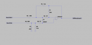
Attached is the LPF (2 per channel and the other LPF acts on inverted signal) feeding a conventional diff amp using OPA627. I would like your opinion on this to see if I would be advised to change to the reference design in the AKM data sheet.
Hope my question is clear and thanks for your help in advance! Just to make things clearer, the caps are 1nF and 470pF.

Last edited:
According to the DS, the minimum AC load is 1k in the default state (HLOAD=0). But the -ve leg of your circuit presents a lower AC load than that due to the opposite phase being presented to the opamp's +ve input terminal. It would be better to equalize the loading on both phases of the DAC's output as per the examples given in the DS.
Thanks Abraxalito!
I was doing a bit of digging and it seems almost to me that the designer would have wanted to make a differential LPF and messed up in the board layout. If that was the case, the attached would be what I assume to be the correct design. Does that make sense and would this comply with the min ac load specs?
I was doing a bit of digging and it seems almost to me that the designer would have wanted to make a differential LPF and messed up in the board layout. If that was the case, the attached would be what I assume to be the correct design. Does that make sense and would this comply with the min ac load specs?
Attachments
The input impedance of the lower leg is 990+714 =1704 ohm
The voltage on the +in of the opamp is 0.419*Uin-, the same voltage is also on the -in of the opamp.
The upper leg:
Across R2 is now 1.419*Uin+ which means the impedance is only 698 ohm.
I think that dac output was designed for a transformer and someone replaced it with this stage
So even if you arrange everything nicely mirrored it won't make a difference
