blu_line said:Hello all,
My diamond output buffer, see PDF, eats output transistors, being Q1,Q4,Q27 and Q30.
I know it has to do with thermal issues. So i tried the following :
Place Q1,Q4,Q27 and Q30 together on the heatsink.
And couple Q6 with Q2 and Q28 with a piece of aluminium.
And the same with Q8, Q3 and Q29.
According to the logical rules this should be a perfect temeparture compensation , cause when Q2 and Q28 heat (and also Q3 and Q29) the current through Q6 and Q8 reduces and so the BE voltage over Q2,Q28, Q3 and Q29 decreases. Fine you should say. Well, when powering-up this immediately pops the power trannies.
So i also tried ; place Q1,Q4,Q27, Q30, Q2, Q28, Q3 and Q29 together on the heatsink. This seems to work.
But i see the quiescent current rise slowly as the heatsink warms-up. So that is not correct either.
And next to that.....
I used series resistors (13 ohm) in the powerline to protect for over-current.
When i remove these i get fireworks also. (i either set-up)
Somebody got some ideas ?
grtz
Simon
Hi, Blu_Line
first forgive my poor command of english.
Based on my own experience, i suggest you to put Q7/Q24 & even Q5/Q25 on heat sink. instead of Q6/Q8.
the reason, reducing current of Q6/Q8 when temperature get rise is more effective than just put Q6/Q8 on heat sink.
reduce the current of pre-driver by Vbe multipiler bias transistor, by put Vbe multipiler bias transistor on the heat sink, NOT by put pre-driver transistor on the heat sink. it is the common principle of push-pull amplifiers.
please do not forget this principle when designing an high power amplifier.
good luck.
I have a feeling of that this topology is not particulary good as you have done here. You must have a realiable temperature stabilisation and predictable bias currents.blu_line said:I was wondering....
I want to set the amp in class A. 1 Amp each transistor
That means, w.r.t. the 10/0.1 formula, i just need 10 mA.
While the BD139/140 is most happy at around 100mA, i could reduce these resistors to 1 vs 0.1. (or less)
Will i need a lot of current to steer it or not ?
grtz
Simon
I have tested myself to increase the difference of the current setting resistors but the truth is that it didn'tr work particulary well. Right now I have 10/2.2 ohms with good results and of cource muchsmaller currents.
Schematic here:
http://www.sjostromaudio.com/hifi_files/qrv/qrv08r0schema_p1.pdf
Are you 100% certain that your Skizlai pair is absolutely stable?
ilimzn said:1) Q2, Q28, Q6, Q8, Q3, Q29 must be on the same heatsink not in contact with the main heatsink.
This was my thinking too, after studying this circuit.
These six should be put together on a medium sized heatsink.
Q6 close to Q2 / Q28
Q8 close to Q3 / Q29
Main big heatsink have only 4 big power transistors: Q1,Q27,Q4,Q30
These four will not effect the bias control.
I would recommend reading Post #7 by ilimzn again:
http://www.diyaudio.com/forums/showthread.php?postid=607889#post607889
Q6/Q8 emitter resistors R9/R10 value depends of how much bias you want in your output.
R9/R10 should not be too high in value because it will make less linearity.
But not too small - because of too much current and power in Q6/Q8.
Each of R26 and R27 could be replaced by resistor + trimpot.
The variable values of these two resistances can be used to set output bias
as well as balance of DC-offset.
Quote:
At first the 47 ohm resistors, R1, R4, R28, R32 smoked.
This can indicate you have not connected BCE pins of output transistors correctly
to the BD140, BD139 drivers.
BD140 should be connected to BD911, BD139 to BD912
and in correct way.
lineup said:
Quote:
At first the 47 ohm resistors, R1, R4, R28, R32 smoked.
This can indicate you have not connected BCE pins of output transistors correctly
to the BD140, BD139 drivers.
BD140 should be connected to BD911, BD139 to BD912
and in correct way.
When mounted on a heatsink, with pins down,
BD139 and BD140 have pins
from left to right: E-C-B
BD911 and BD912 have pins
from left to right: B-C-E
This is tricky to remember!
Hello All,
Thanks for the late postings.
I will read them carefully later.
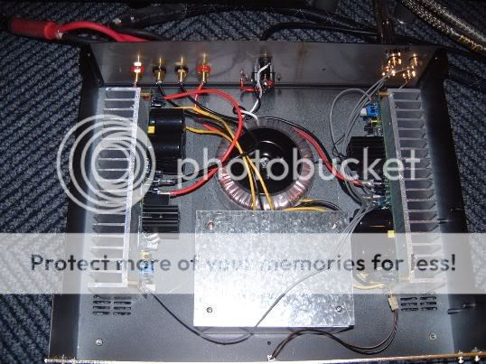
I re-designed the end stage and driver stage. I have put all drivers on one heatsink and the output transistors on the big heatsink.
The circuit is stable.
I have tested it up to +/-30v with +/- 1.4 A.
No problem and i see that the drivers stage is compensating for the temperature.
This week i hope to finish the input section of the amp. I will come back on this
@per-anders
Are you 100% certain that your Skizlai pair is absolutely stable?
[ST : please elaborate ?!
Grtz
simon
Thanks for the late postings.
I will read them carefully later.
I re-designed the end stage and driver stage. I have put all drivers on one heatsink and the output transistors on the big heatsink.
The circuit is stable.
I have tested it up to +/-30v with +/- 1.4 A.
No problem and i see that the drivers stage is compensating for the temperature.
This week i hope to finish the input section of the amp. I will come back on this
@per-anders
Are you 100% certain that your Skizlai pair is absolutely stable?
[ST : please elaborate ?!
Grtz
simon
hi,
I've changed a little bit circuit from my original DC adjustable Power Diamond Output Buffer to this circuit
using On-Semi-ThermalTrak Audio Output Transistors maybe can solve the thermal problem. 🙂
I've changed a little bit circuit from my original DC adjustable Power Diamond Output Buffer to this circuit
using On-Semi-ThermalTrak Audio Output Transistors maybe can solve the thermal problem. 🙂
Attachments
I think this circuit might work.
Keep wires from ThermalTrak diodes short
----------------------------
we need to know what your plans are,
regarding bias of output
is it
low bias Class AB (50mA)
high bias Class AB (200mA)
lower power/current Class A(1500mA)
higher power/current Class A(2500mA)
it is difficult to make more detailed comments until we know this
Value of R9 and R12 (10 Ohm ) may need a change, depending on what you want.
----------------------------
Adjusting R10 and R11 ( 680 ohm ) will change bias. You can use resistor+trimpot for these.
This will increase or decrease current in input transistos.
2SA970/2SC2240 are only 300mW transistors.
I would not use more than 200mW into them, which gives 200/45V= 4.4 mA max current.
Same goes with Q17/Q18.
R17 and R18(100 Ohm) is already putting 7 mA into them.
Gives 7x45V = 315mW - they will probably burn.
I would change to at least 500mW input transistors.
2N5401/2N5551 from OnSemi is 625 mW. This would allow at least 8-10 mA, if needed.
R4 (33kOhm) need to be at least 0.5Watt - can be replaced with two 15kOhm 1/2Watt.
Diamond buffer built.. some questions
Hi, I've built the Thermaltrak version of the diamond buffer (as posted here http://www.diyaudio.com/forums/attachment.php?s=&postid=816573&stamp=1137329785 , with all 2N5551 and 2N5401 as small signal BJTs, MJE15032/33 as drivers and NJL1302/3281, and have some questions:
-To achieve a correct polarization I had to increase, as expected, R9 and R12 to 68 Ohm. Polarization is supply voltage independent and is pretty close to Microcap simulations.
However I'm not sure about the optimal current ratio between driver and output transistor... at the moment is slightly less than 1:3 (25mA drivers - 65 mA outputs). Both drivers and outputs are on the same heatsink.
-Another curiosity is that if I close input to Gnd via a 200 Ohm resistor idle current doubles...and if I short it to gnd current rises further, why ?
Cheers
Andrea
Hi,
I haven't used MJL3281A/1302A to bulid this circuit myself, and I
don't know about their Vbe and Vf, I just "think" that this circuit
will work and solve the thermal problem.
I licenced this circuit to a Taiwan local audio company, and he
made some resistor modifications to adjust the CCS's value lower
than my design, R10/R11 he used 2.74K instead of 680, so the
CCS current should be arround 0.5mA, but he said his output Idle
current near 100mA, the ratio was almost 1:200. 🙂
I have measured several BJTs' Vbe and fined they are with some tolerance, by changing R10/R11 or R9/R12 you can get a Idle
current's value you want. And normally I will suggest arround
200mA and with some heat, 65mA is a liittle bit smaller.
Adding a small value resistor like 100OHM between the input and
the Base of 2N5551 and 2N5401 maybe can solve this problem,
because their Vbe and Hfe MAYBE quite different, some base
current would occur between the input and the Base.
Cheers
mtlin12
Attachments
Hello,
thanks for your reply.
The schematic works as posted with the only change in R9/12 values to achieve sufficient Vbe to correctly polarize the output BJTs.
My prototype was flawed (I had a 2N5551 with collector and emitter inverted... I wonder how could it even work ), but once fixed this problem I must say that none of the problems posted before was there anymore.
DC offset is pretty low (few mV) and bias is stable. I still have to increase it to the 200-250 mA as suggested.
The "Morkai" circuit seems to have a bandwith limitation (higher base resistor and miller cap on the pre-drivers) and settles with a slight bump at power on, while the simpler "Thermaltrak" circuit with the 10 ohm resistor is perfectly silent.
Now some further questions:
- In the Ultima DDPDB R15 and R16 are "after" the pre-drivers while in the other buffers they have a lower value and are between driver and output transistor: which are the motivations for the different choices?
-In these designs I find (Ultima and Morkai) a output relay: since the simple "Thermaltrak" buffer doesn't show startup bump does this mean that the added circuitry needs some time to settle?
I also take the occasion to thank you for posting this nice design.
I haven't listened to it extensively (I just breadboarded a single channel for testing purposes) but it seems to have some good qualities 😀
Cheers
Andrea
thanks for your reply.
The schematic works as posted with the only change in R9/12 values to achieve sufficient Vbe to correctly polarize the output BJTs.
My prototype was flawed (I had a 2N5551 with collector and emitter inverted... I wonder how could it even work
), but once fixed this problem I must say that none of the problems posted before was there anymore. DC offset is pretty low (few mV) and bias is stable. I still have to increase it to the 200-250 mA as suggested.
The "Morkai" circuit seems to have a bandwith limitation (higher base resistor and miller cap on the pre-drivers) and settles with a slight bump at power on, while the simpler "Thermaltrak" circuit with the 10 ohm resistor is perfectly silent.
Now some further questions:
- In the Ultima DDPDB R15 and R16 are "after" the pre-drivers while in the other buffers they have a lower value and are between driver and output transistor: which are the motivations for the different choices?
-In these designs I find (Ultima and Morkai) a output relay: since the simple "Thermaltrak" buffer doesn't show startup bump does this mean that the added circuitry needs some time to settle?
I also take the occasion to thank you for posting this nice design.
I haven't listened to it extensively (I just breadboarded a single channel for testing purposes) but it seems to have some good qualities 😀
Cheers
Andrea
Andypairo said:
.
.
Now some further questions:
- In the Ultima DDPDB R15 and R16 are "after" the pre-drivers while in the other buffers they have a lower value and are between driver and output transistor: which are the motivations for the different choices?
-In these designs I find (Ultima and Morkai) a output relay: since the simple "Thermaltrak" buffer doesn't show startup bump does this mean that the added circuitry needs some time to settle?
I also take the occasion to thank you for posting this nice design.
I haven't listened to it extensively (I just breadboarded a single channel for testing purposes) but it seems to have some good qualities 😀
Cheers
Andrea
ULTIMA- DDPDB
R15 and R16 are "after" the pre-drivers is because I didn't use
voltage regulator for the JFET source-follower stage , so I used
a RC filter instead.
But morkai's Mr.Liu thought the SZIKLAI should be "regulated" as
well, so he suggested using a lower resistor ( for more current)
between driver and output transistor. Acturly I don't know which
is better.
Morkai's IPT has bandwidth limitation, so he doesn't care using
(higher base resistor and miller cap on the pre-drivers), he thinks
that stability of this circuit is much more important, after all it is
an audio merchandise.
Morkai's 25W+25W IRON-AMP ( = a 10dB IPT + 0dB PDB)
You are welcome to use those circuits freely, unless you also want to sell them for business. 🙂
mtlin12
p.s. the stand-by circuit can't work here, don't use it.
Hello mtlin12,
thanks for your valuable replies.
I intend using this diamond buffer as output stage for my Aikido tube preamp.
This preamp is very good but has too much gain for preamp duty, so I dropped the use of a "regular" power amplifier in favour of a unity gain one.
Since I'm a curious guy I dare asking some further questions about your designs: both the Morkai and the Ultima buffers have added circuitry respect to the simpler thermaltrak buffer.
This circuitry includes :
-Q9 and Q10 for proper voltage shifting (Thermaltrak diodes used in the version I use)
-Current sourced led reference for the CCSs (Q14/Q15) and a / vbe multiplier based references for the regulators based on Q7 and Q12
-Adjustable current source to correctly polarize the input buffer (Q8 - 2SK246) and to allow setting of the output current with a single trimpot...
Did I spot the differences correctly or there is something that I miss?
If I got it right using the "thermaltrak" circuit (and setting the current varying 2 resistors) and a preamp with a good "drive" like the Aikido should get pretty close to the more complex design... do you agree?
Cheers
Andrea
This schematic diagram ( page 8 of the LH0033 datasheet ) was the reference of my design.
The speed of LH0033 is very good, But output current still not
enough. So I decided to change its push-pull emitter follower
to a Power DB, that's why I use 2SK246 JFET source follower as
the input stage and use sziklai to compensate the voltage shifting.
2SK246's Vgs is large enough to compensate the Vbe by setting
proper CCS current , but its breakdown voltage (only -50V) is not
enough for +/-38V, so I have to lower its supply voltages. That is
why the circuit looks so complicated, but actually it's quite simple.
I have no ability to design a tube drive, though I'm very interested
in the Italy made PATHOS hybrid amps.
I think Aikido plus a PDB maybe can have the same sound qualities.
mtlin12
🙂
Hi again,
I recently completed the second channel and have further questions: in the prototype I used, at the input, two 100 Ohm resistors between the base(s) if the input BJTs and then a 47k resistor to ground from the middle point of the 100 Omh resistors (and this is my "Input").
With these values offset was about 40-50mV, not that small but still acceptable.
In the following amps I used a 100k instead, to raise input impedance and to extend bandwidth to the lower frequencies (my preamp uses a 0.7uF MKC coupling cap).
However with 100k offset raised to nearly 120mV on one channel and 80 on the other.
At this point I see three ways to overcome this problem:
A- Use a 47k (or lower) from input to gnd and increase the coupling cap of the preamp
B- Remove the 100k to gnd and use 200k from input to +Vcc and a 180k+47k trimmer to -Vcc to set the correct DC offset while maintaining a approx 100k impedance
C- Use the network specified in "B" bypassing its middle point to gnd with a cap (and thus making it a sort of signal gnd) and connecting it to input via a 100k resistor.
What would you use ( btw I accept also a "D" or "E" answer 😀 ) ?
Cheers
Andrea
Hi Andrea,
Did you match your complimentary input transistors for gain? I've run into oscillation problems before and connect the bases directly together these days. 100K to ground will give me + / - 30 mV to ground typically as a worst case.
-Chris
Did you match your complimentary input transistors for gain? I've run into oscillation problems before and connect the bases directly together these days. 100K to ground will give me + / - 30 mV to ground typically as a worst case.
-Chris
Hi Andrea,
D. Try using a 100 ohm trimmer instead of R9 (=68 ohm) and
then trim the output offset.
-mtlin12
D. Try using a 100 ohm trimmer instead of R9 (=68 ohm) and
then trim the output offset.
-mtlin12
Hi,
actually I didn't match the input BJTs. Will match them and if it is not enough I will use a trimmer to eliminate the offset.
Well, as foreseen the best answers were "D" and "E" 😀
Cheers
Andrea
PS Anatech how did you cure you oscillation problems? How are you using this diamond buffer?
actually I didn't match the input BJTs. Will match them and if it is not enough I will use a trimmer to eliminate the offset.
Well, as foreseen the best answers were "D" and "E" 😀
Cheers
Andrea
PS Anatech how did you cure you oscillation problems? How are you using this diamond buffer?
Hi Andrea,
The problem is that a diamond buffer can be very, very fast. You need to ground any heatsinks, decouple (bypass) power supplies and keep supply and signal leads as short as reasonably possible.
If your input transistors starve for current you may get oscillation as well (on signal peaks).
I have been playing with power diamond buffers for a little while. They excel at delivering detail but have limited current delivery without some modification. You have found this out.
Keep going! It's an interesting project.
-Chris 😉
Hi Chris,
I will try to simulate how much does current in the input stage change at loud levels (20Vrms), to see if they do get starved.
I cured oscillations placing a cap between B and C of the pre-drivers, taking example from the "Morkai" circuit.
Which pre are you using with the DB?
Cheers
Andrea
I will try to simulate how much does current in the input stage change at loud levels (20Vrms), to see if they do get starved.
I cured oscillations placing a cap between B and C of the pre-drivers, taking example from the "Morkai" circuit.
Which pre are you using with the DB?
Cheers
Andrea
Hi Andrea,
-Chris
Everything from signal generators to various tube and SS pre amplifiers. Still experimenting.Which pre are you using with the DB?
-Chris
- Status
- Not open for further replies.
- Home
- Amplifiers
- Solid State
- Diamond Output buffer eats trannies (thermal)