I'm looking at a DAC that uses the DF1704 and I'm having trouble finding pin 1. I know the large recessed dot should mark pin 1, but if this is the case on this design, then the pin opposite pin 1 (pin 28) should be LRCIN and this seems to not be connected to anything. I'm not sure how this would be possible, as none of the applications in the manual for this chip show it being operated in this fashion. The only thing I can guess is that pin 1 is somewhere else... sorry for the basic question, but I'm not really sure what's going on here. Package is SSOP-28 and it is marked Burr-Brown (not TI).
luvdunhill said:The only thing I can guess is that pin 1 is somewhere else...
Then it wouldn't be pin 1. How many layers does the board have ? Is there a via under the chip ? A blind via would not be visible on the other side of the board.
More to the point, if the dac actually works, LRCIN must be connected.
Re: Re: DF1704 pin out question
thank you. I didn't even know these things existed 🙂 I suppose it's a multilayer board. Thanks for confirming the pin 1 location. Pin 1 goes to a Xylinx chip, I was hoping that it came from the transport. The transport is a CD/DVD OEM from Matsushita, but I cannot find any model information on the drive that gets any hits on Google.
Looking at the DF1704 datasheet, I was hoping that the Xylinx chip was simply responsible for setting a few of the parameters for the DF1704 chip (this arrangement is given a few times) and that the i2s data would not pass through this chip. This must not be the case.
I'll see what else I can find out on my own 🙂
rfbrw said:
A blind via would not be visible on the other side of the board.
thank you. I didn't even know these things existed 🙂 I suppose it's a multilayer board. Thanks for confirming the pin 1 location. Pin 1 goes to a Xylinx chip, I was hoping that it came from the transport. The transport is a CD/DVD OEM from Matsushita, but I cannot find any model information on the drive that gets any hits on Google.
Looking at the DF1704 datasheet, I was hoping that the Xylinx chip was simply responsible for setting a few of the parameters for the DF1704 chip (this arrangement is given a few times) and that the i2s data would not pass through this chip. This must not be the case.
I'll see what else I can find out on my own 🙂
rfbrw and others:
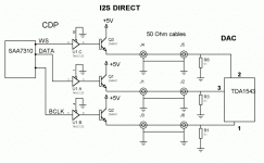
I finally found all three pins by backtracking from the DF1704. They go to a Xilinx XC9536 CPLD. Pin 1 of the DF1704 (DIN serial data input) goes to pin 37 of the CPLD (I/O) and pin 2 of the DF1704 (BCKIN) goes to pin 36 of the CPLD (GTS1 / I/O, some sort of buffer delay perhaps?) and pin 28 (LRCIN) goes to pin 38 of the CPLD (I/O). So, I'm assuming the CPLD takes the data from the transport and probably transforms it in some fashion to prepare it for the DF1704. I'm 99% sure this format is Philips i2s. So, my question is, can I take the output from these locations on the CPLD and pass it to my DAC? I'm not sure how things in the digial realm work, but I'm essentially asking if I can "split" these signals like this and send them to both my new DAC project and the existing onboard DAC (I cannot really "unhook" the existing DAC, so that's why I'm asking as well.. it might also be nice to compare the two).
Thanks so much!
If the DF1704 is in hardware mode, i.e. pin 10 low, the level on pin 3 defines the input data format. It is high for I2S.
As for tapping the signal, it would be best to play safe and buffer the signals before dispatching them anywhere.
As for tapping the signal, it would be best to play safe and buffer the signals before dispatching them anywhere.
- Status
- Not open for further replies.
- Home
- Source & Line
- Digital Source
- DF1704 pin out question