Hi All,
With a bit of hesitation, I'm starting this thread about an onging project of mine. It's been in progress for the past few months and will likely take many more to complete. In other words, this is a work in progress with an unknown end result and issues are guaranteed to occur 🙂.
Preface:
10 years ago, I built my first higher-end DAC off a PCM1794. Used it for a few years mostly with headphones, then gave it away to a good friend of mine to use in his system. Fast forward to last November, I found myself grounded at home for a few weeks. With nothing to do and while going through my archives, I found the design documents of that former DAC and decided to put some effort and design a new (and hopefully better) DAC, taking into account what I've learned in the years since. One thing led to another and I ended up with a lego-style platform with multiple modules that can be mix-n-matched in different ways.
Goals:
- Modular platform - make it possible to use different DAC chips, IV converters/buffers, inputs and/or DSPs
- Favor extensibility wihtout (much)compromising audio quality.
- Open Source and Hardware so that anybody can duplicate, extend and improve.
- Use Open-source/free design tools as well, wherever possible.
With the above said, I introduce DeWille - A high-performance DIY audio DAC.
Current status:
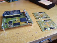
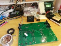
Three hardware-complete modules are available:
- The Base board, which provides power, digital input isolation and physical connectivity between the other boards.
- A PCM1792-based DAC board.
- The Control board, containing:
-- FPGA with some SRAM to implement any kind of signal processing one sees fit. For now, a simple FIFO is planned.
-- A low-jitter clock source
-- A NodeMCU32 COTS board to control all the other devices
Future work:
- Set-up a minimal FPGA implementation that does I2S pass-through
- Write some NodeMCU32 code that set-ups the PCM1792 in the required mode so that I can get some sound out of the system (using a dummy I/V converter)
- Design and build a proper I/V converter board.
I'll periodically post updates here and I'm putting the current schematics as attachments, but the most up to date information will always be available in the project Github page - GitHub - zmeiresearch/DeWille: A high-performance DIY audio DAC
PS. The source code will be MIT licensed - basically, one can do anything he sees fit, except removing the copyright from the source files. The hardware design is licensed CERN-OHL, which requires basically the same.
With a bit of hesitation, I'm starting this thread about an onging project of mine. It's been in progress for the past few months and will likely take many more to complete. In other words, this is a work in progress with an unknown end result and issues are guaranteed to occur 🙂.
Preface:
10 years ago, I built my first higher-end DAC off a PCM1794. Used it for a few years mostly with headphones, then gave it away to a good friend of mine to use in his system. Fast forward to last November, I found myself grounded at home for a few weeks. With nothing to do and while going through my archives, I found the design documents of that former DAC and decided to put some effort and design a new (and hopefully better) DAC, taking into account what I've learned in the years since. One thing led to another and I ended up with a lego-style platform with multiple modules that can be mix-n-matched in different ways.
Goals:
- Modular platform - make it possible to use different DAC chips, IV converters/buffers, inputs and/or DSPs
- Favor extensibility wihtout (much)compromising audio quality.
- Open Source and Hardware so that anybody can duplicate, extend and improve.
- Use Open-source/free design tools as well, wherever possible.
With the above said, I introduce DeWille - A high-performance DIY audio DAC.
Current status:
Three hardware-complete modules are available:
- The Base board, which provides power, digital input isolation and physical connectivity between the other boards.
- A PCM1792-based DAC board.
- The Control board, containing:
-- FPGA with some SRAM to implement any kind of signal processing one sees fit. For now, a simple FIFO is planned.
-- A low-jitter clock source
-- A NodeMCU32 COTS board to control all the other devices
Future work:
- Set-up a minimal FPGA implementation that does I2S pass-through
- Write some NodeMCU32 code that set-ups the PCM1792 in the required mode so that I can get some sound out of the system (using a dummy I/V converter)
- Design and build a proper I/V converter board.
I'll periodically post updates here and I'm putting the current schematics as attachments, but the most up to date information will always be available in the project Github page - GitHub - zmeiresearch/DeWille: A high-performance DIY audio DAC
PS. The source code will be MIT licensed - basically, one can do anything he sees fit, except removing the copyright from the source files. The hardware design is licensed CERN-OHL, which requires basically the same.
Attachments
TI has indicated that people should use the successor http://www.ti.com/product/PCM1792A
On the FPGA signal processing - what specifically would you be doing?
If there's upsampling for example, one option is to make the FPGA window a section of data, the FFT it, adding zero padding and then inverse FFT to make the upsampled stream output.
The FPGA would need enough capability to perform FFT for say 15Hz to 22Khz, then it can inverse FFT and pad on the fly directly to the output stream at the higher rate.
Just been playing with Octave ideas around that yesterday.
Here is an example implementation of FFT on FPGA (although most vendors have optimised IP cores/tiles for this: http://web.mit.edu/6.111/www/f2017/handouts/FFTtutorial121102.pdf
The main thing is ensuring that the FPGA has enough speed and ram to perform the required processing. If the ram is short an alternative is to run external ram however this reduces speed and complicates the designs further.
I would isolate the FPGA output to the next stage too as long as the isolation can keep up.
Last edited:
Yeah, the -A version is pin- and functionally-compatible to the original one. In fact, I have the -A on the two boards.
Regarding FPGA functionality, maybe stating it'll be doing "signal processing" is an overstatement. It's functionality will initially be limited to read the incoming audio signal from whichever input is selected, store it in RAM, then clock it out to the DAC. It'll be used as a glorified input multiplexer coupled with a FIFO. Of course, having an FPGA, it possible to implement anything (as long as it fits), but I don't plan to go beyond some pretty basic stuff - S/PDIF to I2S, supporting the NOS-mode from DDAC and supporting DSD as well.
Putting isolators between the FPGA and the DACs was something that I was considering (and actually did on my previous 1794 DAC) but it will introduce several hundreds of femtoseconds of additional jitter(for most readily available isolators), while the clock generator should be able to achieve sub-100 fs itself. Here my line of thinking is that it’s only the system clock whose stability impacts the analog domain and the rest of the signals are there to just get the data to the DAC.
Yeah, the -A version is pin- and functionally-compatible to the original one. In fact, I have the -A on the two boards.
Regarding FPGA functionality, maybe stating it'll be doing "signal processing" is an overstatement. It's functionality will initially be limited to read the incoming audio signal from whichever input is selected, store it in RAM, then clock it out to the DAC. It'll be used as a glorified input multiplexer coupled with a FIFO. Of course, having an FPGA, it possible to implement anything (as long as it fits), but I don't plan to go beyond some pretty basic stuff - S/PDIF to I2S, supporting the NOS-mode from DDAC and supporting DSD as well.
Putting isolators between the FPGA and the DACs was something that I was considering (and actually did on my previous 1794 DAC) but it will introduce several hundreds of femtoseconds of additional jitter(for most readily available isolators), while the clock generator should be able to achieve sub-100 fs itself. Here my line of thinking is that it’s only the system clock whose stability impacts the analog domain and the rest of the signals are there to just get the data to the DAC.
Move the clocks post isolators, reclock, send clocks back through isolators is
the usual way.
It depends on the type of DAC used. For MB DAC (PCM1704 etc) reclocking
is a benefit. For 1792/4 other DS DACs, theoretically only Mclck is important.
DSD compatibility is a great idea.
TCD