Kenshin said:
why not using a basic emitter follower and put all timing circuit at low side? A piece of logic chip can do all these things well,with fewer pins and more reliability.
By logic chip, were you thinking of something like a programable logic device? I use the CD40106B for just about everything, but I am not thinking the 4000 CMOS family is what you had in mind.
I think that IS actually what he HAD in mind.
If you for instance take an AND gate and feed one input with the signal to be "dead-timed" directly and the other one with its delayed version (through the use of some gates in series or an RC lowpass) you will have an output that will go from low to high with a delay and vice versa immediately.
There are more refined versions possible that include flip-flops.
Regards
Charles
subwo1 said:
Hi. Q29 is the driver stage input. I think you are wondering why Q28 does not serve that purpose so that Q29, Q1, and Q19 can be eliminated. The main reason would involve timing of the MOSFET switching. Such good timing helps to lower distortion, reduce power dissipation in the MOSFETs, and lessen current spikes and associated noise when the MOSFETs switch.
I had thought of trying something with only the three transistors on the right, myself. It would be interesting to simulate both ways to see the differences.
Hi Sub,
Could imposing a delay not be done with less parts? Seems like alot of effort for a simple dead time. Neat idea though.
All the same, do we really want to induce a fixed dead time, that will only help saturate the body diode.. leads to a very short mosfet life.
I've been simulating what you proposed (three transistor driver), my observations:
It serves no usefull purpose, and provides no benefit over the standard driver.
These are complications I believe one would run into with a real implementation of it. In simulation it can be made to work half decent, almost as good as the standard two transistor driver, but not as good.
The biggest problem with all these discrete drivers seems to be gate signal asymmetry, while you can control the low side driver easily enough, the high side driver seems to make the mosfet rocket on.
40106+diode+RC delay,transistor OC output,emitter output voltage follower, DC(not AC)coupled N+P bridge -- This is USTC school robot team's first reliable MOSFET motor driver.
-- by yangyi,2002.(not me)
-- by yangyi,2002.(not me)
phase_accurate said:I think that IS actually what he HAD in mind.
If you for instance take an AND gate and feed one input with the signal to be "dead-timed" directly and the other one with its delayed version (through the use of some gates in series or an RC lowpass) you will have an output that will go from low to high with a delay and vice versa immediately.
There are more refined versions possible that include flip-flops.
Regards
Charles
classd4sure said:
Hi Sub,
Could imposing a delay not be done with less parts? Seems like alot of effort for a simple dead time. Neat idea though.
All the same, do we really want to induce a fixed dead time, that will only help saturate the body diode.. leads to a very short mosfet life.
I've been simulating what you proposed (three transistor driver), my observations:
It serves no usefull purpose, and provides no benefit over the standard driver.
These are complications I believe one would run into with a real implementation of it. In simulation it can be made to work half decent, almost as good as the standard two transistor driver, but not as good.
The biggest problem with all these discrete drivers seems to be gate signal asymmetry, while you can control the low side driver easily enough, the high side driver seems to make the mosfet rocket on.
my three transistor driver/the standard two transistor driver?
does "the standard two transistor driver" means voltage follower?
in my three transistor driver, the first driver is at the low side,so it could also be called "two transistor driver".
and,
what does
"do we really want to induce a fixed dead time, that will only help saturate the body diode.. leads to a very short mosfet life."
mean?
do you mean the dead time should not be fixed,but vary with the gate capicity?
phase_accurate said:I think that IS actually what he HAD in mind.
If you for instance take an AND gate and feed one input with the signal to be "dead-timed" directly and the other one with its delayed version (through the use of some gates in series or an RC lowpass) you will have an output that will go from low to high with a delay and vice versa immediately.
There are more refined versions possible that include flip-flops.
Regards
Charles
Ah yes, I see what you mean.
Thanks.
Kenshin said:
my three transistor driver/the standard two transistor driver?
does "the standard two transistor driver" means voltage follower?
in my three transistor driver, the first driver is at the low side,so it could also be called "two transistor driver".
and,
what does
"do we really want to induce a fixed dead time, that will only help saturate the body diode.. leads to a very short mosfet life."
mean?
do you mean the dead time should not be fixed,but vary with the gate capicity?
subwo1 said:
Ah yes, I see what you mean.
Thanks.
Well the current output I dont' consider part of the driver, so what you have is a two transistor driver, 1= an active pull up/follower, 2= PNP turn off. The other configurations I've tried, only seem to add more parts with no benefit whatsoever.
Why deadtime is bad:
The more dead time you have, the longer inductor current freewheels through the body diode, saturating it. Once saturated it takes a long time for it to be able to recover and block voltage again, then you wind up turning the opposite mosfet on, and it rams current down the throat of a non recovered body diode=shoot through.
You can help that by slowing the turn on, and having a fast turn off, but this isn't a cure, and the slower you turn the mosfet on, the hotter it will run! So it's really not a good cure.
If you can eliminate deadtime, the body diode never conducts! That... is a cure.
So yes, some form of adaptive delay, which, due to propogation delay of the logic circuitry required for that, still allows the body diode to conduct, but not for very long, would help.
Predictive delay (http://focus.ti.com/lit/ds/symlink/ucc27222.pdf)
is said to fully eliminate body diode conduction.
So, THAT, sounds like a cure.
Problem:
IC's that use it like the one I just linked to are only for low voltage drivers, what the hell good is a 12V amp right.
Also, the varying delay seen in either adaptive dead time or predictive deadtime, I think, is something a self oscillating design would naturally compensate for rather nicely.
I've seen the patents and know how they do it, but it looks like a hell of a project for the DIY'r, got to be a simpler way to make a "delay locked loop". By the way, if this interests you, those are words to search for: "DLL or delay locked loop".
Thoughts?
classd4sure said:
Hi Sub,
Could imposing a delay not be done with less parts? Seems like alot of effort for a simple dead time. Neat idea though.
All the same, do we really want to induce a fixed dead time, that will only help saturate the body diode.. leads to a very short mosfet life.
Well, my impression is that adaptive dead time sounds outside the range of the level of simplicity I prefer.
I've been simulating what you proposed (three transistor driver), my observations:
It serves no usefull purpose, and provides no benefit over the standard driver.
I really suspected the three transistor way was not used instead of the two for good reason.
These are complications I believe one would run into with a real implementation of it. In simulation it can be made to work half decent, almost as good as the standard two transistor driver, but not as good.
The biggest problem with all these discrete drivers seems to be gate signal asymmetry, while you can control the low side driver easily enough, the high side driver seems to make the mosfet rocket on.
I know what you mean about the rising bootstrap assembly adding drive to the base of the gate drive input transistor--regeneration.
Kenshin said:40106+diode+RC delay,...
I usually rely on the CMOS gate input capacitance and leave out an external capacitor, depending how much dead time I need, but the principle is the same.
classD4sure:
do you mean the circuit you posted before,with a diode across the PNP transistor's emitter? I don't quite catch it. could you explain it to me?
Anyway,a pull up resistor plus a voltage follower plus the diode is simpler. why not use it? do you want to make a inverting drive at high side,so you need another one?
when the input is already low and the output stays high due to the output coil, the diode turns on,prevent the base of two following transistor be pull under the output(the source of high side FET).
I know what you mean about the rising bootstrap assembly adding drive to the base of the gate drive input transistor--regeneration. [/B]
what do you mean by?
the drive is supported by the voltage on the capicitor--when the output is low,it get charged by 12V PSU at the low side through the diode.
the 12V PSU also powers the low side driver.
no requirement for another boosting PSU.
the total circuit(plus low side & output L )is once simulated,but its not on my computer now.
Attachments
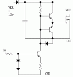
I have a guess on why you use inverting drive at the high side:
the high side circuit has a reference to the output stage,so feedback is involved.
using voltage follower:
Even with no any output device connected, when the input voltage becomes high,the MOSFET turns on,and the output going up, and the input voltage is now low compare to the output,the MOSFET tuning off and the output voltage go low...this negative feedback could cause extremely high frequency oscillations.
use inverting drive at the high side,it will be a positive feedback,causing hystresis and quick switching instead of oscillations.
Kenshin said:classD4sure:
do you mean the circuit you posted before,with a diode across the PNP transistor's emitter? I don't quite catch it. could you explain it to me?
I mean all the discrete drivers discussed.
Anyway,a pull up resistor plus a voltage follower plus the diode is simpler. why not use it?
You seem to understand it fine... why not use it? Simulate it more, you'll see, it is a VERY, VEEEEEEERY weak driver. When I say weak I mean the only way it can work is to achieve a very delicate balancing act between having it so starved for drive that it is just on the verge of not working at all. If it is any more loaded down than that you lose drive voltage to your mosfet (smoke), with any more drive than that.... your drive signals overlap (smoke). So to be honest I think it sucks.
do you want to make a inverting drive at high side,so you need another one?
Inverting? No need. I want a driver with total control over the gate under all conditions, minimal deadtime (non) and zero overlap!
...prevent the base of two following transistor be pull under the output(the source of high side FET).
I'm not sure what you mean?
Kenshin,
Ah yes, the regeneration, an old-timer's term for positive feedback, especially in switching circuits, snaps the high side on, and your reason for including it in the circuit sounds good.
The emitter of the drive input transistor is pulled high along with the MOSFET source by the bootstrap capacitor.
Ah yes, the regeneration, an old-timer's term for positive feedback, especially in switching circuits, snaps the high side on, and your reason for including it in the circuit sounds good.
what do you mean by?
The emitter of the drive input transistor is pulled high along with the MOSFET source by the bootstrap capacitor.
if not with the diode,the b will be pulled to GND quickly,so the transistor's bc junction will be positively biased.
to make things worse,if not the follower ...the gate pulled to GND...and the source is on high voltage output...smoking...
to make things worse,if not the follower ...the gate pulled to GND...and the source is on high voltage output...smoking...
subwo1 said:Chris,
Thanks for the warning about the non-inverting MOSFET driver. I am sure I was lax in forgetting a previous warning I had received about that method.
I think this diode is the one.
subwo1 said:Chris,
Thanks for the warning about the non-inverting MOSFET driver. I am sure I was lax in forgetting a previous warning I had received about that method.
I think this diode is the one.
Oh wow, you guys had me right confused there! zzzzzzzzzzzzzzzzzz
I didn't realize you were talking about that circuit again, sorry.
It may be happening in the famous L6203 motor drive.It can run WITHOUT boosting. so the gate driver must be not coupled with the output.
2 years before,i'm using it in a robot. when the MCU go wrong,the L6203 broke --even with a small current lamp serialed at the power. The chip first leaked,the motor turning strangely,than the current go up slowly...after 1 minuit...
now imagine,it may be this.
2 years before,i'm using it in a robot. when the MCU go wrong,the L6203 broke --even with a small current lamp serialed at the power. The chip first leaked,the motor turning strangely,than the current go up slowly...after 1 minuit...
now imagine,it may be this.
...The chip first leaked,the motor turning strangely,than the current go up slowly...after 1 minuit...
Indeed, reverse breakdown can cause internal hot spots and then failure.
Regarding the reverse recovery problem: In the near future there will be output devices specially aimed at class-d amps. They are in fact already available though not in small quantities.
Oother example that isn't specifically targeted at class-d is a newer version of the IRF540:
http://www.irf.com/product-info/datasheets/data/irf540z.pdf
It's body diode has a reverse recovery time in the range of good fast-recovery diodes.
The other solution would indeed be an adaptive dead-time control. I have a Tripath patent somewhere dealing exactly with that but I haven't read it yet.
Regards
Charles
- Status
- Not open for further replies.
- Home
- Amplifiers
- Class D
- Development of a "reference" class D starting point