To help the OP, I would suggest good design practice rather than elaborate measurements, for reasons I've already mentioned. If datasheet performance is the target, then following the manufacturer's design instructions would definitely help in making it there. Nevertheless, if one has any difficulties with that, he/she may simply replicate the manufacturer's typical / recommended design or alternatively the evaluation board design / layout for the relevant product to obtain "claimed" performance.In order to help out the OP here may we ask which measurements would you suggest the OP perform in order to cover all possibilities presently known to science?
If a measurement is absolutely desired, then a good start would be feeding the system with "zero" input.
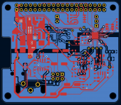
Hi all, thanks for the comments so far. I have laid out the PCB now - see attached. Couple of additional comments:
Once constructed, I will measure whatever I can with my equipment - my DAC has THD+N around -105dB (it's from here).
- The input side of the 3V3 regulator is attached to digital ground. One of the outputs is at the top of the resistor dividers that provide the reference for the diff. inputs - the bottom of those dividers is analog ground. The other output is used to power the ADC and also as a pull-up for EN and the I2C address pins.
- The analog side is furthest from the Pi header, so that return current from digital components should not pass through the analog ground plane.
Once constructed, I will measure whatever I can with my equipment - my DAC has THD+N around -105dB (it's from here).
Attachments

Updated schematic?
Maybe wiser to put the SMPS on the bottom side, off in one corner, and all the sensitive analog stuff on top (including the ESS voltage regulator) on top and away from the SMPS corner?
Regarding opamp bypass cap layout you might read the post at: https://www.diyaudio.com/community/...apacitor-simulation-model.382329/post-6944464 ...then next few posts after that by KSTR. He explains his thoughts about some layout issues. Actually you might want to study the whole thread including the links.
Last edited:
Thanks for the link! I need to watch those youtube videos on decoupling.
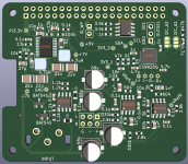
I was a bit unsure where to put the ESS voltage regulator, but now that you mention it, it probably needs to move. If I move the flash chip to the bottom side, and put the ESS voltage regulator on the top side, where the flash chip is now, it might work better.
What's the motivation to move the SMPS to the bottom side? I would prefer to avoid putting the inductors and 22u caps on the bottom side of the board.
I will attach new schematic later.
You might want to check out this thread in general and the specific post about 9311 robustness:It will be pretty similar to the datasheet circuit, using ESS's own ES9311 regulator to power the ADC chip
https://www.audiosciencereview.com/...io-analyzer-project.36234/page-2#post-1312445
syn08 used to be a member here but got banned for some reason.
I posted about similar issue with ES9822PRO here. I've had 3 ES9822PROs fail unexpectedly without any clear reason. ESS dacs seem to be robust though.You might want to check out this thread in general and the specific post about 9311 robustness:
https://www.audiosciencereview.com/...io-analyzer-project.36234/page-2#post-1312445
Maybe ground/power plane areas inside the board can help act as electrostatic shielding of radiated SMPS noise. That's how Allo ended up laying out Revolution DAC which used SMPS. Those guys are very measurement oriented, so I expect they could measure some benefit. IME ground planes can be useful for shielding as well.What's the motivation to move the SMPS to the bottom side?

If the power supply is cornered away, it would be easier for the currents to enter and return through short paths that do not interfere with the rest of the sensitive circuitry. Plus, if the SMPS is on the opposite side (and you have ground / power planes like bohrok2610 recommended), there would be some shielding due to these planes (as already mentioned by Markw4).What's the motivation to move the SMPS to the bottom side? I would prefer to avoid putting the inductors and 22u caps on the bottom side of the board.
However, if these planes are occasionally interrupted by routing and / or plated through-holes / vias, then it is not guaranteed that the return currents would exactly trace the supply currents physically. So, it's best to keep the routing to the outer layers (only), and avoid TH components as far as possible. Besides, these planes are often necessary to get decent performance from an on-board SMPS.
I would recommend putting inductors on the bottom (along with the SMPS), as they appear to be drum-cores that have an open magnetic flux path. Though this helps provide a large air-gap and high saturation currents, the flux lines entering / leaving the gap can induce stray voltages in nearby conductors. The ground/power planes falling in between would, once again, at least partially shield the sensitive components electromagnetically. A core with a closed magnetic path would have its flux more contained but then drum core is the popular choice in such small power applications.
Thanks for explaining your thinking everyone.
I do need to have a look at the cost of 4-layer board. I actually didn't consider it as I assumed it would be too expensive. This board is aimed to deliver decent performance for low cost - hence the use of NE5532 (not OPA1612) and ES9820 (not ES9822PRO). But I should validate my assumption.
The SMPS is only powering the op-amps, which means it is very low power. The location of the SMPS is currently as close as possible to its input source (5V from top left pin of Pi header), with the analog section as far away as possible. Another thing I had in mind was that large components on both sides might be an issue since they might fall off during reflow, but I can just hand-solder the inductors.
I suspect moving SMPS to other side of a 2-layer board will only be a marginal improvement, but it's unquestionably best practice, so I will just do it anyway.
I will post updated layout & schematic when it's ready.
You may not realize how much your forum friends are trying to save you from making a dud first time around. Maybe we should let you fail, but what good is that if it makes you give up after one try?I suspect moving SMPS to other side of a 2-layer board will only be a marginal improvement...
Are you saying I am crazy to try to do this with a 2-layer board? Or that I am crazy not to move the SMPS to the back side of the board (which I am about to do)?You may not realize how much your forum friends are trying to save you from making a dud first time around. Maybe we should let you fail, but what good is that if it makes you give up after one try?
No. You could probably get some A/D going even if it was buzzing and distorted, unless maybe you started having mysterious ESS chip failures or something. But, you are getting many man-years of experience in way of advice to assist you. Sometimes it feels like hearing that advice can be an annoyance. Like you don't want to believe this stuff is important. You may not know it but there are people selling commercial products that sound pretty awful (I will not name names at the moment), and they have a lot more experience than you.Are you saying I am crazy...
I am just trying to understand if it is worth building a 2-layer version (with the SMPS circuitry on the backside as recommended) and measuring the performance to see if it meets the desired goal?No. You could probably get some A/D going even if it was buzzing and distorted, unless maybe you started having mysterious ESS chip failures or something. But, you are getting many man-years of experience in way of advice to assist you. Sometimes it feels like hearing that advice can be an annoyance. Like you don't want to believe this stuff is important. You may not know it but there are people selling commercial products that sound pretty awful (I will not name names at the moment), and they have a lot more experience than you.
Okay. The answer is you need 4-layers to do a 16-bit data converter properly even if it has no SMPS. 24-bit converters on 2-layers I would not call crazy. Ignorant, maybe, except you were advised, strongly advised, as I recall. So ignorant can't be right either.
Certainly, but I was not sure whether the advice was targeted to achieve the stated design goals, or to milk every last dB. If I achieve my goal of -100dB THD+N in stereo using a 2-layer board, when the datasheet states -108dB for this chip, have I done it properly? I hope you understand my point - I am not asking these questions because I don't believe that performance will be better with the suggested changes - I'm just trying to understand whether a compromise to lower cost is feasible. Perhaps I should try both 2-layer and 4-layer, and compare the results!Okay. The answer is you need 4-layers to do a 16-bit data converter properly even if it has no SMPS. 24-bit converters on 2-layers I would not call crazy. Ignorant, maybe, except you were advised, strongly advised, as I recall. So ignorant can't be right either.
I will also add the possibility to externally supply the op-amps instead of using SMPS, as it's very easy but I forgot to do it.
The problem is that THD+N is pretty meaningless in terms of whether the thing sounds awful or if it sounds okay. So why do we keep going back to THD+N?
Correct me if I'm wrong but isn't what you really want is for it to sound okay, not awful? The -100dB THD+N thing is just your way of trying to quantify that?
Correct me if I'm wrong but isn't what you really want is for it to sound okay, not awful? The -100dB THD+N thing is just your way of trying to quantify that?
4-layer boards are getting very low cost, very close in price to 2-layer. Even the price of 6-layer has been coming down. Have you checked prices at JLCPCB?
Also, its not clear at this point if you are going to be satisfied with the sound and or measurements you get from the first design iteration. What may add to cost is having to do multiple iterations until you get something acceptable to you. OTOH, if you follow good advice your chances of keeping cost down because of fewer board iterations will be much better. To get the most value out of a board iteration its worth taking the time to think about setting it up so you can perform a few different experiments with each board version. You may be able to figure out a whole lot with only one board design. Maybe.
Have you thought about any strategy to help prevent damage to the ESS parts? Maybe that's something we should talk about?
Last edited:
Since you have components and routing on the these layers, there's not going to be enough scope for an unbroken ground pour that is necessary to get good performance. A 2-layer ground plane PCB works well only if all (or most) of the components / routing are on the same side, which is clearly not your case.I am just trying to understand if it is worth building a 2-layer version (with the SMPS circuitry on the backside as recommended) and measuring the performance to see if it meets the desired goal?
Do you know how they failed?I posted about similar issue with ES9822PRO here. I've had 3 ES9822PROs fail unexpectedly without any clear reason. ESS dacs seem to be robust though.
What protection did you use on the analog inputs of the ADC? Did you use diodes or similar to protect against the currents from an overdriven op-amp driver stage?
- Home
- Source & Line
- Digital Line Level
- Designing ES982x-based ADC - feedback wanted