I assure you, I don´t trust simulations that much. But when it comes to at least getting a circuit to work I believe simulation is a good way to determine things that don´t work.
And of course, why would I even build a prototype if I completely think that sims will tell everything?
Listening is a big part of any development process, both amps and even more so speakers.
Tomorrow it´s back to the workshop and test this weekends sims in practice. So far they haven´t matched that good.....
Once I´m done I´ll post the real measurements etc.
🙂
syn08 said:
Indeed, the balance is very delicate, one good reson why HEC never really made it outside the DIY world.
http://www.synaesthesia.ca/OP-stage.html
Nice amplifier, syn08 🙂
It is one amplifier like that I'd like to try to build.
Some time, maybe.
Right now, I have not the place/workshop to do something more than my smaller breadboard circuits experiments.
But I probably will move and get me better audio workshop facilities.
When I do, one serious amplifier like in your article would be my choice.
Hope you can keep your website stuff online, for at least 5-10 years more.
Audio regards 😎
Lineup - Lineup Audio Lab
Lineup community website, members only

Too bad! It seems I have to abandon the Cordell circuitry, I simply cannot get it to reduce distorsion. I did find a optimum setting for the resistors, but the second and third overtones only read the same level as without the EC. Any other setting increased distorsion.
At 10 watts into 4 ohms and 200 mA idle/device resistive load I get:
H2 about -82 dB
H3 about -95 dB
Seems the simplest way to improve performance further is to mount larger heat sinks and crank up the idle current. I also did try the sliding bias arrangement, and it actually reduced distorsion 3-4 dB, but the amp then suffered from thermal instability, probably due to the diodes in the bias circuit. Basically I´m back to square one again....
At least the amp sounds good. 🙂 I think maybe because the odd overtones are generally lower than the even ones.
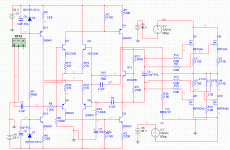
12k for the CCS tail gives only 310uA through each half of the LTP.
This seems very low. Why so low?
Why 5401 &2240 in the LTPs?
8.9mA through the To92 VAS seems high. Why?
C2*R8 is too wideband cf. C3*R10?
Is R18 the speaker load?
Why is R8 different from R16?
Where is the RF input filter?
This seems very low. Why so low?
Why 5401 &2240 in the LTPs?
8.9mA through the To92 VAS seems high. Why?
C2*R8 is too wideband cf. C3*R10?
Is R18 the speaker load?
Why is R8 different from R16?
Where is the RF input filter?
Why is R8 different from R16?
R8 forms the input impedance of the noninverting input, as I see it R16 forms with R10 the negative feedback, about 30dB if I calculated correctly. Of course it's also frequency dependent.
Have fun, Hannes
but unmatched values force the base currents and offset voltage out of balance creating unnecessary output offset that varies more with temperature.
Andrew, the low current through the input transistors is because I used some delicate Rohm-devices earlier, the superlinear 2SC2389 and 2SA1038. I plan to use the 2SA970 and 2SC2240 but didn´t find the 2SA970 in my Multisim. The current ahs to be set for lowest noise depending on which transistors will be used.
For now, the actual prototypes use 2N5401/5551 all over.
8.9 mAmps through Q1 and Q2 is a bit high for the TO92´s used now, but I plan to change these into bigger ones and increase the current to about 15 mAmps to improve slewrate. The FETs has quite a lot of input capacitance, and if a third pair is added it would be good to have som extra drive current available.
Actually, the original design had a emitter follower drivers stage, but as the need for Gate-current isn´t that high I omitted it. Simpler circuit i always nice.
R18 is the load. R9 is different from R16 because it actually doens´t matter too much. I put R9 there as a protection in case the input devices fail. (limit the current to the source)
However, I simply forgot to add a RF-filter at the input! Will do! And also set the input lowpas to the same freq as the nfb lowpass.
🙂
set the input high pass as the bandwidth limit.
The AC across the NFB cap should be as near zero as possible. It should NOT act as the bandwidth limiter.
A complication as you increase the LTP current is a complementary increase in input offset current. Your unmatched inv & ninv resistors will become more significant as offset current increases.
The AC across the NFB cap should be as near zero as possible. It should NOT act as the bandwidth limiter.
I think you will find that it gets quieter with more LTP current. But, you will have to substantially reduce the collector load resistor value.The current ahs to be set for lowest noise depending on which transistors will be used.
A complication as you increase the LTP current is a complementary increase in input offset current. Your unmatched inv & ninv resistors will become more significant as offset current increases.
Thank you Andrew, I see your point now.
@Rikard: how come that the 2sc2389 is no longer sold as low-noise part? In old datasheets it's specifically advertised as low-noise part including the charts, in the new datasheet it appears to be the identical part - but without any noise specs.
Worse quality control? Using a different manufacturing process would change other specs as well I guess.
Have fun, Hannes
Hmm, the 2SC2389 is probably still possible to buy. It´s a very good input device.
Andrew, you mean reducing the collector load of the input devices will reduce noise? or did you mean Q1 and Q2?
I can´t understand why different values of the inv/non inv resistors will have any significant effect on performance?
Both hold the same potential at all times.
Andrew, you mean reducing the collector load of the input devices will reduce noise? or did you mean Q1 and Q2?
I can´t understand why different values of the inv/non inv resistors will have any significant effect on performance?
Both hold the same potential at all times.
Rikard,
😀
right, the gate current is not very high, can be considered as zero. Most importantly, less parts means lower costs.Actually, the original design had a emitter follower drivers stage, but as the need for Gate-current isn´t that high I omitted it. Simpler circuit i always nice.
😀
Rikard Nilsson said:Too bad! It seems I have to abandon the Cordell circuitry, I simply cannot get it to reduce distorsion. I did find a optimum setting for the resistors, but the second and third overtones only read the same level as without the EC. Any other setting increased distorsion.
At 10 watts into 4 ohms and 200 mA idle/device resistive load I get:
H2 about -82 dB
H3 about -95 dB
Seems the simplest way to improve performance further is to mount larger heat sinks and crank up the idle current. I also did try the sliding bias arrangement, and it actually reduced distorsion 3-4 dB, but the amp then suffered from thermal instability, probably due to the diodes in the bias circuit. Basically I´m back to square one again....
At least the amp sounds good. 🙂 I think maybe because the odd overtones are generally lower than the even ones.
just a quick question here...... what is the distortion from your sig gen? the numbers say your distortion is in the triple digits, about 0.008%. i'd begin looking at magnetic coupling between the P/S wires and the input stage or VAS as these are often overlooked. still that's pretty darn good distortion.
increasing the LTP current usually moves the operating point of the input transistors to quieter operation.Rikard Nilsson said:reducing the collector load of the input devices will reduce noise? or did you mean Q1 and Q2?
I can´t understand why different values of the inv/non inv resistors will have any significant effect on performance?
Both hold the same potential at all times.
But, when you increase the LTP current, you must reduce the collector load value to match the voltage across the VAS.
The two inputs to the LTP, inv & ninv, should be exactly the same. i.e. the voltages and impedances should be equal.
if you unbalance an impedance (or resistance) then you force the LTP to operate with unbalanced voltages.
Match impedances on both sides of the LTP and then voltages start to match and thermal effects also match. For that reason I usually put the same collector load on both legs of the LTP, to match the Vce and thus the dissipated power.
unclejed613 said:
just a quick question here...... what is the distortion from your sig gen? the numbers say your distortion is in the triple digits, about 0.008%. i'd begin looking at magnetic coupling between the P/S wires and the input stage or VAS as these are often overlooked. still that's pretty darn good distortion.
Thanks, I haven´t yet measured the distorsion from the signal generator itself, but it is probably way lower than the amp. If I measure the amp at lower power, 1 watt into 4 ohms, I get :
H2 = -95 dB
H3 = -100 dB
But surely, some of it comes from the generator itself. And your´re probably right about the magnetic aspects. For example, the large cap in the NFB divider is a MKP, kind of big size. Replacing it with a higher quality electrolytic would reduce the area that could pick up noise and magnetic fields.
I will replace the transistors as a next step, and try the 2SA970 and 2SC2240 for the input, and some sligthly heavier ones for the VAS/predrivers. Mounting them onto the heat sink could improve things maybe, at least thermally although it´s very stable right now.
The thing that annoys me the most is that I know most of the remaining distorsion comes from the output, and I really would like to get some error correction or sliding bias arrangement to work properly.
Rikard, the 2SC2389 is still an active part. I was just wondering why it is no longer a low noise part; that could be interesting for you as you of course want a low noise input LTP.
Have fun, Hannes
Have fun, Hannes
h_a said:Rikard, the 2SC2389 is still an active part. I was just wondering why it is no longer a low noise part; that could be interesting for you as you of course want a low noise input LTP.
Have fun, Hannes
It probably is a low noise device still, but as the quality of transistors generally is better than a few years ago I bet there are even better ones if we look around. I have the original transistors lying around, but wanted to test a few others. So one of the prototypes run 2SC2389 and 2SA1038 and the other one 2N5551/5401. I cannot see or hear any major differences, I measured approx 1 dB better H2 value for the 2SC2389, but that could be just higher bias.
Would driving the FETs from a lower impedance (such as a source or emitter followers) improve distorsion?
adding a true driver stage must surely improve performance.Rikard Nilsson said:Would driving the FETs from a lower impedance (such as a source or emitter followers) improve distortion?
i was looking at the schematic, and noticed your compensation cap C9 goes from the VAS to the inverting input of the diff amp. shouldn't it go to the base of Q2? if so it should be matched by another one from B-C of Q1
unclejed613 said:i was looking at the schematic, and noticed your compensation cap C9 goes from the VAS to the inverting input of the diff amp. shouldn't it go to the base of Q2? if so it should be matched by another one from B-C of Q1
I originally had caps from B to C of Q1 and Q2, but Lumba suggested that this solution would be better. He´s probably right, but the value had to be reduced to avoid a bandwidth reduction. I guess stability has improved, at least from what I can see in the sims.
- Status
- Not open for further replies.
- Home
- Amplifiers
- Solid State
- Designing amp with 2SJ201/2SK1530