so you prefer some cfb (sziklai) output arrangement
from this miller capacitance issue point of view
interesting, unclejed
always something new to learn 🙂
from this miller capacitance issue point of view
interesting, unclejed
always something new to learn 🙂
it's useful if you're expecting capacitive loads. also for the same reason, i really don't like QC output stages, since the capacitance is in parallel with the load on the top half of the waveform, and in series on the lower half. i use mostly EF outputs, but considering the capacitance dilemma, i'll certainly try CF output stages in my design.
capacitive loads
they are no pure dc resistance, are they?
😀
and can mock up one amplifier operation really
i have made one clone amplifier
a discrete transistor version of one capacitance load stable commercial op-amp chip
it was amazing performance 😎
the squarewave oscilloscope simulation did show nothing
but pure clean squares!
Into whatever capacitive loads I added ...
Very unusual!
so sure, there are ways, to improve amplifier behavior into such difficult loads 🙂
unclejed613,
the CFP has several unique features, a highly efficient superior "error correction" with unbeatable accuracy as working in a direct and fast manner, without a single additional part - desirable properties in audio (unlike what certain commonly preferred harmful solutions offer). Drain /collector drive is just another one.
the CFP has several unique features, a highly efficient superior "error correction" with unbeatable accuracy as working in a direct and fast manner, without a single additional part - desirable properties in audio (unlike what certain commonly preferred harmful solutions offer). Drain /collector drive is just another one.
Lumba Ogir said:Rikard,
frankly, I am having considerable difficulties finding anything I like about this design. The correction occurs over many stages and unlinear diodes strongly reducing its accuracy, on the whole probably doing more damage than good. Numerous other topological annoyances and massive negative feedback effects will keep the subjective qualities at a less than mediocre level.
Lumba Ogir, the error correction is almost a rip-off from the original Cordell circuit, so I have nothing to say if you don´t like it.
The input and predriver setup is simplicity itself:
Two current sources, Q11 and Q12 feeds a diff amp each which in turn operates the predrivers Q1 and Q2. Everything in class A except the FETs. Very simple, and quite effective from what I can see in the sims.
Could you please specify what it is you don´t like?
About the diodes in series with the FET gates, any nonlinearities in the audio range could be clamped with caps in parallell, so that should not be a problem. Their task i simply to reduce the drive voltage for the FETs enabling the EC network to operate properly.
Besides, a few mV of nonlinearity from the diodes is not much compared to the much larger ones from the FETs themselves. According to simulations, the output and EC is what really works well in this design, I got 0.003% THD into 4 ohms at 10 watts using only the output stage, without global feedback! I think it´s great.
🙂
Rikard Nilsson said:
According to simulations, the output and EC is what really works well in this design,
I got 0.003% THD into 4 ohms at 10 watts using only the output stage,
without global feedback!
I think it´s great.
🙂
Rikard.
This is great, even for a simulation using ideal voltage sources.
I do not think even Lumba would need to worry, too much 😉
This also shows, that the ideas of Robert Cordell still holds even some years later, today.
And this is very normal for a basically good audio design idea.
Now, you should really try to add one measured & simulated transformer
and so get one more realistic power supply into circuit.
This will be a good additional sim test.
To see what happens when you set up using non-ideal power supply.
Regards Lineup
See attached image:
Attachments
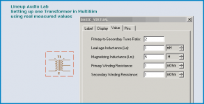
Well, the simulated supplies are not realy ideal, I have added 2 volts of 50 Hz ripple in the the output supply, but of course, a transformer would be in place. Also the filters to the input and predrivers.
🙂
🙂
lineup wroteThis also shows, that the ideas of Robert Cordell still holds even some years later, today.
And this is very normal for a basically good audio design idea.
Credit where it is due. Hawksford published the basic circuit in 1981. The use of NFB to reduce distortion and the use of PFB to generate gain are ideas that predate this by many decades, originally used in valve circuits.
There is still much to be learned from valve designs. 🙂
Rikard Nilsson said:Well, the simulated supplies are not realy ideal, I have added 2 volts of 50 Hz ripple in the the output supply, but of course, a transformer would be in place. Also the filters to the input and predrivers.
🙂
Rikard,
How about measuring the PSRR? You can do this by putting an ac voltage source in series with the psu line and then plotting the ratio of Vout to Vpsu vs f.
Brian
what i want to look at, both in simulation and real components, is what the "open loop" output resistance is like for CF vs EF. it's the output resistance interacting with a capacitive load that causes oscillation as well.since it's usually beyond the frequency limits of the input stage, it's the "raw" output resistance since there's no feedback available to lower the output impedance.
Rikard Nilsson said:Well, the simulated supplies are not realy ideal,
I have added 2 volts of 50 Hz ripple in the the output supply,
but of course, a transformer would be in place.
Also the filters to the input and predrivers.
🙂
2 volts of pure 50 Hz sinus onto pure DC-voltage ideal source
.. it is not one ideal supply for power amplifier
.. at least not if you use same voltage source for Input stage + VAS + Power Output
But it is much more ideal
than a more realistically simulated virtual Power Suppply.
100/120 Hertz ripple would be even more realistic, '
mostly 😀 😀
Lineup
.
my self use 90% of all cases,
Separate transformer + voltage source for Output stage
... in power amplifier Circuits
.
All that have seen my power amplifier schematics,
of my own design/idea
knows this well
.
Actually, the only one that has told me,
at this board
that he uses separate supply for each stage
is one guy:
JOHN CURL
Not any the of other so called gurus 😀 😀
🙂 You may have a little guess, why I do so.
It is not to reduce ripple mainly.
It is not 100 Hertz ripple I fear the most.
Because this can be dealt with rather well with capacitor filtering.
It is to break all 3 supply rails between the output and input.
V+ V- and Reference GND
Why?
Have a guess 😉
Currents works in CIRCLE .. CIR-CUIT.
Same supply, same circuit.
Feed-Back current works in CIRCLE
Has to return to same place via rails.
================
😎 You think there is no Feed-Back via V+ and V- rails.
I say there is .. in a real Cir-Cuit.
it is not your own intended Feed-Back
This is a level, a degree, of un-wanted, un-intended feed back
from The Non Ideal Real Power Supply Line.
At least, me Lineup, call this feed-back.'
As it is AC currents from Output to the stages before = Input/vas
A disturbance feedback that only can create distortion
.. in the real world.
.. in the real PCB .. no matter how nice PCB Layout
Lineup
lineup said:
100/120 Hertz ripple would be even more realistic, '
mostly 😀 😀
🙂 You may have a little guess, why I do so.
It is not to reduce ripple mainly.
It is not 100 Hertz ripple I fear the most.
Because this can be dealt with rather well with capacitor filtering.
It is to break all 3 supply rails between the output and input.
V+ V- and Reference GND
Why?
Have a guess 😉
Currents works in CIRCLE .. CIR-CUIT.
Same supply, same circuit.
Feed-Back current works in CIRCLE
Has to return to same place via rails.
================
😎 You think there is no Feed-Back via V+ and V- rails.
I say there is .. in a real Cir-Cuit.
it is not your own intended Feed-Back
This is a level, a degree, of un-wanted, un-intended feed back
from The Non Ideal Real Power Supply Line.
At least, me Lineup, call this feed-back.'
As it is AC currents from Output to the stages before = Input/vas
A disturbance feedback that only can create distortion
.. in the real world.
.. in the real PCB .. no matter how nice PCB Layout
Lineup
the eipple waveform is a 100/120Hz rounded sawtooth.
this is why it's important to strive for as good a PSRR (power supply rejection ratio) as possible, as well as good filtering and bypassing of the power supply. using current sources and current mirrors helps with the PSRR, and large caps and plenty of bypass caps helps with the power supply ripple. if you really wanted to go completely wild with a design, you could have power supply rails that are regulated, but that increases your transistor count as well as your heat sink requirements. you could use very stiff regu;ation, but your output power would hit a "brick wall" at the rail voltages you are set to, or looser regulation do you could keep some dynamic headroom. a third option would be a tracking regulator for a class H-like amp. i don't think it could really be called class H because you wouldn't be commutating a second set of output devices.
Rikard,
your design comprises a large number of unlinear plain stages having wide operating area and high gain. As shock treatment, multiple negative feedback loops applied bringing about deteriorating compensation. Count on excessive dynamic distortions due to poor bandwidth, serious phase errors and heavy overdriving. The distortion figures you are getting are easily achievable with any kind of topology and tell nothing about the sound, certainly nothing favourable.
Welcome to this great site.
Thank´s Lumba, I´m looking forward to see you suggestions of improvements then! 😉 I did some further testing today, but the EC networks seems to be next to inactive, at least when it comes to improving the distorsion figures. I got about -85 dB for the second overtone when cranking up the idle. I went kind of overambitious at one point, and blew the fuse in series with the 300 watt transformer primary! Good to know the Toshiba devices were ok taking about 500 watts of dissipation without failing....I´m thinking of replacing all the feedback resistors in the EC with trimmers, and simply try my way forward to the best settings. I find it a bit tedious that the thing simulates so beautifully, but doesn´t impress me "live". The sound is actually very nice anyways, but it has always been. No hum, no hiss, no strange "dirt" in the top treble range, and rock solid bass! If I cannot get the Cordell circuit to work properly, the next step is to try something slightly simpler, a dynamic bias circuit that moves the switch off point of the "non active" device further into the operating area of the acitve one. The crossover distorsion is kind of spread over a larger voltage range, and should in my opinon be easier to correct with ordinary NFB. Something like this:
Attachments

Rikard,
it`s much cleaner now!
A few simple suggestions, I would:
insert emitter resistors for the input devices, say 220Ohm.
change R8/R16 to say 15KOhm (and R10 accordingly).
omit the capacitor parallel with R16
limit the gain of the VAS by resistors from collector to ground, say 15KOhm.
change the CCS to ring of two type.
rearrange C11/C8 from collector to the inverting input.
Thanks Lumba!
It´s cleaner simply because it´s a different approach, the Cordell circuit is replaced with a simpler bias circuit. Otherwise, it´s the same amp.
I understand from your suggestions you want to reduce open loop gain. I´m not sure I agree with that. I know some people are "allergic" to NFB, but in my opinion it´s a good thing. Actually, massive amounts of NFB (as long as it is stable of course) is what I looked for with the design. I did have emitter resistors at first, but omitting them reduced distorsion. Less components and less distorsion at the same thime sounded ok to me. 🙂
Also, that´s why the predrivers are operated as current sources. THe collectors "see" a infinite impedance, making the gain close to the hFE of the transistors themselves. Since everything seems stable I can´s really see the problem with the high open loop gain.
However, rearranging the caps from the predriver outputs to the inverting input is interesting. Maybe this would allow me to cascoding the predrivers, and get rid of the Miller effect. This could reduce distorsion some more. If it becomes unstable, your idea of limiting the gain could do the trick.
Reducing the value of the feedback resistor is ok with me, in practice this might make the amp more immune to outer interference from the supply or similar. The drawback is that the cap in series with R10 has to be larger, and this means I have to use a electrolytic instead of the MKP I have now = possibly more distorsion.
But reducing the grounding resistor at the input seems like a bad idea. Why would I want to lower the imput impedance to 15 k?
The resistors only task is to keep the input potential at ground level, which it already does very well. If the current sources driving the input transistors are well balanced there is no problem keeping the DC offset very small.
I´ll be back! 🙂
Now I have done some more simulating, and it looks like I´m going back to the Cordell solution. Optimizing the output stage alone showed how delicate the resistor values are. Definately going to use trimmers and try to find the optimum values by testing and looking at the spectrum analysis at the same time. Also, I found that it´s possible to omit one of the transistor pairs, letting the feedback/bias transistors control the drivers directly. I was able to get even better distorsion figures this way!
Bob, if you read this, any comments about that?
Further, thanks to Lumba, the amp is now stable with cascoded predrivers Q1,Q2 and Q13, Q22. Freq comp cap C8 feeds back to the inverting input of the differential input. Can´t tell if this improves distortion, but it is likely. Most transistors now operate as current coupled units, voltage swings are low except for Q13, Q22 and later.
I added emitter resistors again, as suggested by Lumba, but distorsion figures get worse. So the values are quite low, but maybe stability will improve in practice.
Rather than uploading pictures, the .ms8 file is available here:
http://www.autostock.se/download/?FILE_ID=Circuit5 HEC.ms8
Please feel free to develop this thing further if you like! 😉
PS. Maybe trying the IRFP240/9240 devices would be the next step as the Toschibas aren´t available in the MultiSim 8.
Rikard Nilsson said:Optimizing the output stage alone showed how delicate the resistor values are. Definately going to use trimmers and try to find the optimum values by testing and looking at the spectrum analysis at the same time.
This is how I did it when I encountered the same issue (post PCB, unfortunately). Indeed, the balance is very delicate, one good reson why HEC never really made it outside the DIY world.
http://www.synaesthesia.ca/OP-stage.html
Ahh, nice to see somebody else trying this as well! 🙂
Quite a beast you have there.....
A few things I noticed though:
R75, R76 form a voltage divider together with R88. I assume you did this to lower the drive voltage to the FETs. According to Cordell himself this is not very good, as it enhances the conductance droop making it harder for the EC to correct the stage. That´s why I use diodes intead. Maybe in practice it doesn´t have that big influence, can´t tell yet.
What voltage do you use at the input?
Rikard,
your blind trust in simulation data regarding distortions misleads you completely, preventing you from designing good sounding amplifiers. Hopefully, you will realize that some sunny day.
your blind trust in simulation data regarding distortions misleads you completely, preventing you from designing good sounding amplifiers. Hopefully, you will realize that some sunny day.
- Status
- Not open for further replies.
- Home
- Amplifiers
- Solid State
- Designing amp with 2SJ201/2SK1530