[NOT For Help]
Switching power supplies can be implemented in many different ways using different output voltage control mechanisms. The simplest form is a power supply that achieves output voltage regulation indirectly using the transformer principle. In this case, the output is a *multiple of the input voltage.
The general basic operating principle of switch-mode power supplies is the following.
An cored inductor is energised by passing current through it but avoiding magnetic saturation of the core. This stores an energy equal to:
In a cored inductor, the stored energy exists as long as a sustaining current flows in the coil. A switching power supply, turns off the magnetising current and redirects the output to the inductor into the output smoothing capacitors which hold many times the inductor's maximum energy. For the inductor to charge the output smoothing capacitor, it must develop a voltage that is equal and opposite to the voltage on the smoothing capacitor. This forces the inductor to adjust a current decay rate according to the relation v = -L(dI/dt). The fact that an inductor has the ability to adjust to any dI/dt means it can develop any voltage across its terminals. This is what controls the output voltage of a switch-mode power supply. A control circuit is used to direct this inductor energising-deenergising phase, so that, the output voltage remains within the accepted tolerance.
As mentioned earlier, the simplest form uses transformer based regulation and does not use an inductor.
Switch-mode power supplies come in two families: flyback converters and forward converters. A flyback converter uses the transformer as an inductor while a forward converter uses a transformer as a transformer and an inductor in the output section. A forward converter does not always need a transformer depending on the input and output voltages.
* multiple: some refer to this as a percentage
Switching power supplies can be implemented in many different ways using different output voltage control mechanisms. The simplest form is a power supply that achieves output voltage regulation indirectly using the transformer principle. In this case, the output is a *multiple of the input voltage.
The general basic operating principle of switch-mode power supplies is the following.
An cored inductor is energised by passing current through it but avoiding magnetic saturation of the core. This stores an energy equal to:
Code:
E = LI^2/2

This relation can derived from first principles using v = -L(dI/dt).
An increment of energy is dE = v.I.dt. Using both of these
equations results in an integration which leads to the first quoted
relation.As mentioned earlier, the simplest form uses transformer based regulation and does not use an inductor.
Switch-mode power supplies come in two families: flyback converters and forward converters. A flyback converter uses the transformer as an inductor while a forward converter uses a transformer as a transformer and an inductor in the output section. A forward converter does not always need a transformer depending on the input and output voltages.
* multiple: some refer to this as a percentage
[NOT For Help]
A flyback converter uses the transformer as an inductor...
No. A flyback inductor isn't a transformer, because:
1.- the output voltage isn't related by the turns ratio and in a transformer there is, and..
2.- there isn't simultaneous transfer of energy between inductors, in a transformer, there is.
Lloyd Dixon suggest the term "Mutually coupled inductor" over the "transformer" for a flyback power transfer device.
The innards of switch-mode power supplies.
At the heart of any advanced switch-mode power supply, there is control circuitry which continuously monitors the output voltage and current. This is usually achieved using pulse-width modulation of a square wave signal. The latter is generated by a triangle wave generator, an error amplifier (an opamp) and a fast comparator. The error amplifier is filtered to avoid unwanted oscillation of the entire circuitry. It must not respond too fast and it must not repond too slowly as the output may move out of what is tolerated.
The control circuit:
The pulse width drives a driver circuit which is capable of very quickly discharge and charge the gate capacitance of a power MOSFET that delivers the current to either a transformer or directly to an inductor. It is very important that the driver circuit is quick and efficient as this can result in a power MOSFET not turning on and off quickly enough absorbing power that makes a power supply infecient and is a danger to the MOSFET itself as it can overheat it to destruction.
At the output, the voltage is differentially amplified comparing it to a reference voltage. The amplified version of this signal is fed to a comparator which compares a triangular wave and this signal. Depending on which of these signals is higher the output of the comparator clamps between 0V and full comparator output.
In the case of a forward converter an additional primary coil is used to return the magnetic energy stored in the transformer's core back to the input DC power rail. Some energy may be returned back by another smaller coil to power the internal low voltage circuitry.
At the heart of any advanced switch-mode power supply, there is control circuitry which continuously monitors the output voltage and current. This is usually achieved using pulse-width modulation of a square wave signal. The latter is generated by a triangle wave generator, an error amplifier (an opamp) and a fast comparator. The error amplifier is filtered to avoid unwanted oscillation of the entire circuitry. It must not respond too fast and it must not repond too slowly as the output may move out of what is tolerated.
The control circuit:
Code:
output sensing signal--->|----------------|
                         |error amplifier |-|
voltage reference------->|----------------| |
                                            |
                               |------------------|
triangle wave form oscillator->| comparator       |
                               |------------------|
                                   |
pulse width modulated outputAt the output, the voltage is differentially amplified comparing it to a reference voltage. The amplified version of this signal is fed to a comparator which compares a triangular wave and this signal. Depending on which of these signals is higher the output of the comparator clamps between 0V and full comparator output.
In the case of a forward converter an additional primary coil is used to return the magnetic energy stored in the transformer's core back to the input DC power rail. Some energy may be returned back by another smaller coil to power the internal low voltage circuitry.
Problems of switch-mode power supplies.
Aggressively switching on and off an inductor, is asking for high voltage flyback discharges, if care is not taken to guarantee an inductor's current never drops too suddenly. Together with this, if an inductor has more than one separate coil or tappings on one coil, leakage fluxes setup by a coil used to energise an inductor or transformer, at the point of turning off a magnetising current, suddenly drop to zero causing severe ringing or high voltage spikes. This energy has to be directed away from the switching MOSFET as it adds to the input rail voltage. Usually, this is done using resistor-capacitor snubber circuits. The snubber's characteristics should not disrupt the overall characteristics of the switching MOSFET plus transformer/inductor. Additionally, there is the issue of capacitance between the energising coil and the other secondary output coils. The energy in this capacitance has also to be taken care of. There are methods of minimising this capacitance by using a foil between the primary and secondaries. The foil has to be grounded to the power rail ground.
Another problem is when output sensing is not properly done. Voltage transients must be filtered off not to disrupt the functioning of the control circuitry. The control voltage sense terminal must only see voltage averages which do not cause the output to move out of tolerance.
Due to high frequency switching switch-mode power supplies produce parasitic signals which have to be cleared from the output and mains input. This is done using capacitors, ferrite cores with a few turns and voltage dependent resistors.
Last edited:
edbarx - "Voltage transients must be filtered off not to disrupt the functioning of the control circuitry. The control voltage sense terminal must only see voltage averages"
Well, that's certainly debatable, depending on the type and purpose of the power supply design. You're posting in "The Lounge" - is debate what you're looking for?
Example, some power supplies I'm familiar with you could send an audio signal to digitally, connect a speaker (through a DC blocking cap) and they'd play music...for 7 bit input resolutions, anyway. They were designed to move their DC output voltage value about quite quickly, like a DAC with explicit settling time specifications. You had to be careful with remote sense filtering, to keep the voltage command dynamic response performance intact.
Like ASi industrial PSU's? They use a choke to maintain the DC and modulate over it the communication protocol.

The fact switch-mode power supplies are extremely efficient and flexible, and the fact on this forum, switch-mode power supplies are considered too complicated to be considered as a DIY project, motivated me to create this thread. Yes, discussion would be most welcome to break this fear of this 'new' technology.edbarx - "Voltage transients must be filtered off not to disrupt the functioning of the control circuitry. The control voltage sense terminal must only see voltage averages"
Well, that's certainly debatable, depending on the type and purpose of the power supply design. You're posting in "The Lounge" - is debate what you're looking for?
I do not know whether I understood correctly. In a class D amplifier, which is a pulse width modulator that can produce positive and negative pulses, an audio signal is used to modulate the pulse width but there is no feedback from the output into the pulse width modulator. Is what you mention something similar to this?Example, some power supplies I'm familiar with you could send an audio signal to digitally, connect a speaker (through a DC blocking cap) and they'd play music...for 7 bit input resolutions, anyway. They were designed to move their DC output voltage value about quite quickly, like a DAC with explicit settling time specifications. You had to be careful with remote sense filtering, to keep the voltage command dynamic response performance intact.
When there is a complete feedback loop from the output to the pulse width modulator, any voltage instability in the loop will present itself in the modulated output: that has to be avoided if stability is to be maintained.
I designed a flyback SMPS and a LLC SMPS.
I learned a lot from it.
flyback are good for varying input voltages while givin ga constant outptu voltage.
LLC like a constant input voltage but act more like a transformer.
I used a PIC micro to generate the LLC frequencies.
The trick is getting the LLC frequencies right.
The upper one isnt too critical but the lower one is.
If it becomes too low the transformer can take a lot of current and blow the mosfets.
LLC SMPS employ an LC resonator in series with the pulse modulated current feeding the power stage and output. Its aim is to present the switching MOSFET a sine wave instead of a square wave which helps reduce MOSFET turn-on and turn-off losses. However, this is a limitation which also puts more stress on the output high speed diodes. The voltage, being sinusoidal, can only conduct current into the output smoothing capacitor near its peak. I prefer a square wave switching arrangement. MOSFET turn-on and turn-off times should be used to determine an optimal switching frequency. This should not be too high to avoid having too much power lost in switching on and off. It should also be high enough to allow for decently sized inductors and transformers.
Using a high switching frequency is a temptation as it might boost one's ego, but efficiency requires that the switching loss per cycle be kept low. If T_on (turn on time) + T_off (turn off time) << T_on_per_cycle (time MOSFET is hard on), this can be met.
Using a high switching frequency is a temptation as it might boost one's ego, but efficiency requires that the switching loss per cycle be kept low. If T_on (turn on time) + T_off (turn off time) << T_on_per_cycle (time MOSFET is hard on), this can be met.
Designing a fixed frequency switch-mode power supply is simpler compared to designing a variable frequency power supply.
Let us calculate the inductance required for a switching frequency of 100kHz, a maximum duty cycle of 10%, a maximum switching current of 50A and a primary DC voltage of 300V. The power supply is assumed to be of the flyback type and the output voltage to be 30V DC. So, we have this cycle: energise inductor ---> let inductor dissipate its energy into an output capacitor .
For this energising phase to be useful and not destructive, all this energy has to be passed on to the output capacitor. Otherwise, the inductor will saturate causing MOSFET failure. The reason for this is, when the inductor does not get rid of all its stored energy the core is still magnetised. Each subsequent cycle will add more to this unreleased inductor energy, until the inductor's core is saturated, and the inductor starts behaving like an uncored inductor causing the MOSFET to blow, because of excessive drain current.
Let us assume there is a turns ratio of 10:1 in accordance with an primary voltage of 300V dc and a secondary of 30V pulsating.
Note 1: In designing the actual switching stage, care must be taken to account for MOSFET turn on and turn off times.
Note 2: As the calculation show we are using only 20% of th entire cycle for our switching operation. If this is the maximum, this is very unoptimal. This means, the primary inductance is not the best choice. However, if instead of 30V output, we were to opt for a 5V output, the flyback phase would be extended by a factor of 30/5 = 6 times, i.e. 6μs. With this change, we are using 1μs + 6μs = 7μs => 70% of the entire cycle which is better and guarantees the inductor's core never saturates.
The mathematics may be tedious, but it is tolerable considering one can design and build a custom power supply.
Let us calculate the inductance required for a switching frequency of 100kHz, a maximum duty cycle of 10%, a maximum switching current of 50A and a primary DC voltage of 300V. The power supply is assumed to be of the flyback type and the output voltage to be 30V DC. So, we have this cycle: energise inductor ---> let inductor dissipate its energy into an output capacitor .
Code:
Vdc: 300V
Duty Cycle: 0.1
Max MOSFET current: 50A
Output voltage: 30V dc

For an inductor, the induced EMF is given by:
v = -L.dI/dt (dI/dt being the rate of current increase of decrease)

For a maximum inductor current I and an on pulse of t seconds, we have:
I = (dI/dt).t

=> I = (v/-L).t

t is the on time, which works out to be given by:
t = (1/f).d      d being the duty cycle

Substituting:
I = (v/-L).(1/f).d
=> I = -v.d/(Lf)

Rearranging the equation:
LfI = -vd
=> L = -vd/(fI)

In our case, this evaluates to:
L = -(-300)x0.1/(100000x50)
=> L = 6e-6H or in sub-multiple form 6μH.Let us assume there is a turns ratio of 10:1 in accordance with an primary voltage of 300V dc and a secondary of 30V pulsating.
Code:
Since, for any inductor L:
L ∝ N^2  i.e. the inductance is proportional to the
square of the number of turns.

If we take 'a' as the constant of linear proportionality:
L = a.N^2

For the primary 6μH:
a = L/N^2
a = 6e-6/N^2
=> a.N^2 = 6e-6

For the secondary, Ls would be:
Ls = a.n^2  where n = 0.1N
=> Ls = a.(0.1N)^2
=> Ls = a.N^2.(0.01)
=> Ls = 6e-6.(0.01)
=> Ls = 6e-8H

Again, for any inductor:
v = -L.(dI/dt)

For a back electromotive force (EMF, that is, reactive voltage)
of v, the rate of current decay is:
dI/dt = -v/L

The initial secondary flyback current, J, is the turns ratio
times the maximum switching current. This is a
consequence of the Principle of Conservation of Energy.
The flux in the core is an energy form which takes time
to convert itself into other forms.

Therefore:  J = I.turns_ratio
=> J = 50x10 = 500A

Calculating the time for this current to drop to zero:
For a secondary voltage of 30V:

dI/dt = -v/L
=> dI/dt = -30/6e-8
=> dI/dt = -5e8A/s (Amperes per second)

For an initial current of 500A, the time required is:
time_required = J/(dI/dt)
=> time_required = 500/5e8
=> time_required = 100e-8 = 1μs (1 micro second)
Note 2: As the calculation show we are using only 20% of th entire cycle for our switching operation. If this is the maximum, this is very unoptimal. This means, the primary inductance is not the best choice. However, if instead of 30V output, we were to opt for a 5V output, the flyback phase would be extended by a factor of 30/5 = 6 times, i.e. 6μs. With this change, we are using 1μs + 6μs = 7μs => 70% of the entire cycle which is better and guarantees the inductor's core never saturates.
The mathematics may be tedious, but it is tolerable considering one can design and build a custom power supply.
Your approach is naive. The following may also be subject to errors.
For strictly discontinuous operation with a single or two switch flyback you assume 50% duty cycle at minimum input voltage to allow for reset. The minimum input voltage is set by design of the input filter and smoothing. Let's say you have 110VAC and use a voltage doubler. Peak is 311V but you design for say 250V. It depends on how you size the filter capacitors for ripple and if required a half cycle line drop out.
Pick your required output power. 100W. Assume an efficiency of 80% and your input power becomes 120W. The average input current from 250V will be 120/260 or 0.46 amps. The input current waveform is a 50% duty cycle triangle wave so it's peak is 4 times the average or 1.85A. Design for a 20% overload and you set the current limit in your supply at 2.3A. This is also the peak primary current. The RMS primary current will be 0.41 times the peak for 50% duty cycle or 0.76A
If your operating frequency is 100KHz 50% duty cycle will be a 5uS on time. During this time your primary is set through 250V. The primary inductance will be given by...
Lpri = Vin.Ton/dI = (250 x 5E-6)/2.3
Lpri = 540uH
You assign equal, half the available, winding area to the primary and secondary(ies). You estimate the required core area product from...
Aw.Ae = Lpri.Ipk.Irms/Bpk.J.Kw.Kcu.Ki
Aw is the bobbin winding area.
Ae is the core effective area.
Lpri is your target primary inductance.
Ipk is the peak primary current.
Irms is the RMS primary current.
Bpk is the peak/suturation flux density of the core.
J is the operating current density of the winding.
Kw is the primary utilisation of the winding area.
Kcu is the wire utilisation of the winding area.
Ki is for margin isolation.
Bpk may be loss limited but assume 300mT
Kw is 0.5 Half assigned to primary.
Kcu is 0.7 for round wire.
Ki is a guess of 0.8. 20% loss for two times 3mm margins 6mm total.
J is 2E6 assuming a 40C rise and convection cooling.
Some of these numbers are subject to wide variations depending on the application. In particular the number chosen for J. For a simple inductor operating with 20% ripple current 4E6 would be a reasonable value. In this case winding currents are discontinuous and the AC losses go up as a result of penetration and layer effects so I have used 2E6.
Aw.Ae = (540E-6 x 2.3 x 0.76)/(300mT x 2E6 x 0.5 x 0.7 x 0.8)
Aw.Ae = 562E-9
Assuming Aw = Ae results in Ae = 75mm^2
The minimum number of primary turns you need is given by...
Npmin = Lpri.Ipk/Bpk.Ae
Npmin = 540E-6 X 2.3A/300mT x 75E-6
Npmin = 55
https://ferrite.ru/uploads/pdf/products/etd/etd_29_16_10.pdf
Looks fairly close and is available gapped to 200nH per root turn. 50 turns would give an Lpri 500uH which apparently would violate my original sums but these things are variable. It's all an approximation but the idea of the approximation is to quickly home in on a possible solution. Once there or close you iterate around that solution to check as to its viability.
Unfortunately that includes consideration of other things and, for the moment, I am not going to do that. I would tentatively be happy to put 100W through an ETD29 core in an offline application using a discontinuous flyback topology.
Last edited:
Naive is a derogatory term, most probably, you mean, my approach is over-simplified. In that, you are absolutely right.MorbidFractal said:Your approach is naive. The following may also be subject to errors.
In my calculation no account has been taken of the saturation flux of the inductor's core, the flux leakage, the mutual inductance coupling factor, the MOSFET's turn-on and turn-off times, the effects of high speed switching on inductor resistance,...
The are other important factors to consider which have been left out in my simplified account. These are high voltage ringing due to switching and methods to keep such ringing under control and the prevention of interference signals from reaching the load circuitry and the mains.
Last edited:
You may interpret naive as being derogatory but it is to the point when used to describe your design approach.
The criteria you use indicates a single switch flyback convertor with a target output of 750W but you make no mention of this.
It does not matter what other throw away statements you use or other concerns you introduce to excuse yourself. If someone were to follow your guidance they would rapidly end up in a serious amount of pain.
I still couldn't find the core of this discussion. Some isolated concepts. 750W for a flyback is only for a mad designer. Let's see what happen further.
If by core you mean the 750W figure the design as proposed uses a peak inductor current of 50A, a primary inductance of 6uH and switching frequency of 100KHz. 0.5LI^2 x Fsw gives you 750W. The other approach is 50A peak triangle at 10% duty cycle is an average of 2.5A from a 300V supply which again gives 750W. The numbers work but as you suggest it is mad.
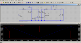
The attached schematic is a forward converter power stage and switching stage. The screenshot is an LTSpice simulation. The red trace has a part with a finite postive gradient, which also happens with a real circuit I built for self learning purposes several years ago.
According to my logic, which may be flawed due aging and inevitable death of neurons, on MOSFET turn on, the voltage on the primary should be equal to the power supply voltage remaining that value until the MOSFET is turned off. At turn off, the flux starts to drop causing the induced voltage to change direction, which adds with the power supply voltage raising the MOSFET's drain voltage to twice the supply voltage. Then, it 'mysteriously' starts dropping uniformly for a period of time until the MOSFET turn on again.
Can anyone, with less dead brain cells, explain this to me.
Thanks for your patience and your time.
Attachments
What you are seeing is the primary magnetising inductance resetting via the clamp winding to the input supply. If your duty cycle is less than 50%, it has to be to allow for this reset assuming equal setting and resetting voltages to avoid it entering saturation, then the magnetising current falls to zero before the switch turns back on again and you see the fall in the drain voltage. With an ungapped core as would be used in such a convertor your winding inductances will be greater than the 100uH you have used. Guess 40 turns on 2000nH then perhaps 3.2mH. In respect of your secondary side snubber you will see ringing due to parasitic capacitances both with magnetising and leakage inductance. Generally you model leakage as a series inductance in the primary or secondary. The leakage inductance will give high frequency ringing the magnetising inductance low frequency. Such ringing will be apparent at various periods during the switching cycle dependent on which junction is reverse biased or nominally open circuit and they can be dealt with individually.
For those who want to study switching power supplies, LTSpice has several ready made schematics using ICs. Browsing through several of these circuits, my impression is, LTSpice examples/jigs folder focuses on low voltage outputs that are not suitable to power amplifiers. However, one can still learn a lot studying them. For higher voltages, there are ready made ICs that simplify SMPS desging considerably. I will consult a SMPS design handbook I acquired about thirty years ago to give a list of chips one can use, but readers have to keep in mind, these are old chips from almost two decades ago. Needless to state, one can still try to find modern chips which provide similar and far improved functions.
In general, an SMPS power stage is the the part of the circuit which is subjected to short pulses of heavy currents. This means, parasitic inductances and capacitances become very important. Parasitic inductance is reduced using various methods one of which is reducing the distance between the switching power MOSFETS and switching transformer/inductor.
Please note, this very basic explanation is NOT sufficient to provide the knowledge and expertise necessary to successfully design and build a powerful SMPS.
Post Scriptum:
In 1992 I built a variable voltage SMPS based on the chip L296. The original schematic is NOT my work. The circuit is very simple and supplies a voltage from 5V to 30V at a current of 0A to 4A. The chip provides soft start and short circuit protection. The datasheet for the chip has a working circuit together with a PCB layout. The chip is by ST Microelectronics.
Last edited:
Digitally Controlled Switch-Mode Power Supplies:
Besides using an analog controller, an SMPS can be effectively controlled using a digital controller. In this setup, an analog to digital converter continuously reads the instantanesous output voltage. These readings are then processed by software algorithms to calculate a duty cycle for the next pulse or sequence of pulses. An algorithm can be coded to sense short circuit conditions and to simulate soft starting. Additionally, an algorithm can be coded to sense and prevent ringing of the output.
For DIYs a microcontroller has to be capable of accepting custom coded algorithms as an algorithm is much more than setting a value to affect an output or an input.
Using a digital controller does not free an SMPS designer from properly designing MOSFET driver circuits. The switching transformer/inductor will still need careful design to avoid damage by parasitics.
This approach is simpler to understand but costlier.
- Home
- Amplifiers
- Power Supplies
- Designing a switch-mode power supply.