Hmm according to the formula provided by pacificblue a 47 µF cap would filter -3db at ~4.13 Hz. Is this right or not?
That is right.
The only responses that I can give to you is that AndrewT repaired my amplifier in near live time via internet posts and the resulting values are:
2.7k feedback-shunt resistor series to 242.0047uF.
The 220uF electrolytic is individually disadvantaged by 3.3R that I added at its groundside.
The amplifier has remained in service for years and continues to ward off competitors.
And the other response is that -3db is extremely bad distortion when gain is applied--please use a -0db reference point in order to dodge noise.
Your functional capacitor value will be bigger. Any variation from theoretically ideal capacitor will make it bigger again.
Is the error that we're seeing called "wrong side of knee voltage"?
Last edited:
Add a resistor between the input pins. A value between 100k and 1meg will help against popping noises.
Add an X or Y rated capacitor between transformer pins 1 and 4. A few nF will do. Add 100 nF ceramic capacitors between transformer pins 5 and 6, 7 and 8 and between rectifier pins 3 and 4.
Should the "popping resistor" be placed before or after the pot if I use one?
Are 0.1 µF 250V caps fine between T1 and T4? 5PCS 0.1uF 250V 104J CBB Metallized Film Capacitor | eBay
What are the functions of the different caps?
The caps between rectifier pins 3 & 4 are snubbers right? However I stated in the OP:
I'd like to keep the design as simple and straightforward as possible. Not only will it be easier to build, but I might also have a small chance of understanding what the hell I'm doing.
I've been reading Peter Daniel's threads until my head hurts and intend to make the power supply somewhat similar to his GC's.
I'd like to keep the design as simple and straightforward as possible. Not only will it be easier to build, but I might also have a small chance of understanding what the hell I'm doing.
Like tube rolling, like op-amp rolling, plugging a power op-amp into a support circuit meant for a much different power-op amp is a non-optimized, non-specific use that does not promote understanding; but, instead, that sort of thing promotes confusion. That can make a headache for sure.
The LM3875, LM3876, LM3886, LM4780 non-inverting gainclone is intensely bright and clear with annoying hot mids and so using extra large caps like 1500uF directly at the chip swamps the problem with power noise at the expense of performance and thermal management.
The LM1875 does not require this circuit.
A poor quality power circuit increases the difficulties of thermal management, which is seriously counterproductive to such a small chip; therefore, the 47 Labs gaincard copies are showing you what to avoid. Read the reviews. Notice the heat.
I am grateful that LM1875 is different than those.
Last edited:
You know, its possible that LM1875 is within range of the sturdy regulator chips, for the clean fresh sound of good power.
Its a small expense but it blocks a lot of unwarranted variety from the transformer, thus simplifying design. Nick Whetstone at Decibel Dungeon has a lot to say about regulated power for your amplifier.
One of the more fascinating things he has to say about regulators is that a little added cap changes the noise performance of the regulators and concurrently, at the same time frame, the heat output from the amplifier falls back down to the range of normal. I suspect, but do not know, that these two things occurring at the same time, could be closely related.
The discrete regulators and related capmulti do not seem to effect heat, and I suggest that this is a difference in HF output. For using regulator chips, perhaps a filter could be added to the amplifier so that it would refuse to amplify the HF output of regulator chips, thus accomplishing the same drop in heat output. . . on purpose. It is worth exploring, or you can dodge it by using the published discrete regulator.
I guess, but do not know, that individual regulators per left channel and per right channel could give you the bigger Dual Mono (monobloc) presentation, yet with the purchase of only one reasonable transformer.
Last edited:
I shall quote the man himself:
Source: Building a Gainclone chip amp with a regulated power supply (PSU).
I've failed to draw the bridge rectifiers correctly on more than one occasion.
In all seriousness though I like the concept of a regulated supply in theory but this is my first "real" electronics DIY-project (I've fiddled around with the Arduino for a few weeks before this) and I hope to keep it somewhat simple so I can maintain an understanding of what's going on. It goes way over my head sometimes and I'll probably have to meditate for a week on all that's been discussed here today. And yes, it would also add significant cost to the project for the extra caps and heatsinks needed for the regulated supply.
Let's keep this simple and if all goes well I can raise the bar for the next project. I have two LM3886 chips just sitting there waiting...
I'll assume that you know how to make the rectifier bridges and connect them to the transformer. If you don't then may I suggest that you make a 'basic' GC first and come back to this section when you have it working OK.
Source: Building a Gainclone chip amp with a regulated power supply (PSU).
I've failed to draw the bridge rectifiers correctly on more than one occasion.
In all seriousness though I like the concept of a regulated supply in theory but this is my first "real" electronics DIY-project (I've fiddled around with the Arduino for a few weeks before this) and I hope to keep it somewhat simple so I can maintain an understanding of what's going on. It goes way over my head sometimes and I'll probably have to meditate for a week on all that's been discussed here today. And yes, it would also add significant cost to the project for the extra caps and heatsinks needed for the regulated supply.
Let's keep this simple and if all goes well I can raise the bar for the next project. I have two LM3886 chips just sitting there waiting...
Okay, then, in addition to the NFB cap booster patch, I have a power circuit patch for you.
Since the optimized power circuit is different for all op-amps you can see why the power circuit specific to a LM3875 gainclone does not instantly transfer to all other op-amps.
Therefore, we can band-aid patch the power circuit on your schematic by paralleling the textbook value for LM1875, 330uF with whatever larger value you want, such as 1500uF from your schematic, resulting in 330uF//1500uF Panasonic FC.
This should adapt the gainclone power circuit to fit LM1875.
It is possible that you may prefer 470uF instead of the 330uF in the example above, so be sure to acquire both options.
A pot before the cap will have the same effect as the resistor. If you use a pot, skip the resistor.Should the "popping resistor" be placed before or after the pot if I use one?
No. For capacitors that are connected to mains, you need to use X or Y rated capacitors. X or better are required between L and N, Y are required from L or N to PE, and they are better than X.Are 0.1 µF 250V caps fine between T1 and T4?
They are different kinds of snubbers that act against voltage peaks produced by inductive components during switching. Caps 1 and 2 are for the transformer, caps 2 and 3 for the rectifier.What are the functions of the different caps?
Rectifiers are switching on and off 100 times per second on 50 Hz mains or 120 times on 60 Hz. You won't hear the effect directly, but probably in a comparison with or without the second and third cap, because cleaner supplies make life easier for the amp.
The ommission of the first and second cap can lead to popping noises in audio components in the neighbourhood each time you switch the amp on or off.
Concerning the power supply, the datasheets shows 100 nF right at the LM, 100 µF on the PCB and does not mention the big smoothing caps next to the rectifier, because the author assumed the latter to be common knowledge. 100 µF on board is a minimum value, so if you put the big smoothing caps right on the PCB, you can skip those. However in that case it would be wise to use some smaller caps, like 10 µF between the 100 nF and the big caps.
Regulated power supplies on a power amp are like a speed limiter on your car to assure you cannot drive faster downhill, than uphill.
My apologies. Earlier, I should have said capacitive multiplier.Regulated power supplies on a power amp are like a speed limiter on your car to assure you cannot drive faster downhill, than uphill.
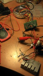
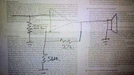
I built a one-channel test circuit with minimal components. No pot, 22k at input to ground, 22k feedback, 560R to ground. 1500 & 0.1uF decoupling. I get ~26.5Vdc at the rails, ~10mV offset at output with speaker connected but no sound whatsoever. No hum, no popping, nothing. Could my chip be faulty? All connections are okay as far as I can tell. Are there any other measurements I could do to shed some light on what might be wrong?
edit: The chip doesn't even get warm fwiw.
edit: The chip doesn't even get warm fwiw.
Attachments
Last edited:
Perhaps some technicolor will help resolve the wiring mess?
http://www.diyaudio.com/forums/chip...-hifi-lm1875-amplifier-board.html#post1514985
This is not my very best project because it contains the error of omitting the NFB cap and the error of slightly too high voltage. . . so you might not want to propagate those two aspects. However, the phenolic board layout is quick and good.
That's a nice little walkthrough but I fail to see how it would help my case? Fwiw I have a bunch of different sized universal boards and I'll design the layout once I can decide on the schematic (and enclosure) to use.
Let me restate my question: If the chip is fried, wouldn't it be more probable to measure either 0V or 26.5V at the output instead of a steady 10.3mV? And if so, it's possible that the chip is ok, I just need to figure out where the problem lies.
Or are you trying to say that it has to do with the wiring?
can you show these components on the schematic?I built a one-channel test circuit with minimal components. No pot, 22k at input to ground, 22k feedback, 560R to ground. 1500 & 0.1uF decoupling.
can you show these components on the schematic?
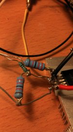
Resistors connect to power ground via signal star, speaker terminal connects directly to power ground.
Attachments
You are right that a fried amp will show rail voltage at the output in most cases, and the 10 mV you get, appear to be the DC offset of a healthy IC.
Your first step should be to measure continuity from the LM's pins to all other points tosheck for bad solder joints.
The next step should be to make sure there are no shorts in the circuit. Put some isolating material between the LM's pins and cover the unisolated wires, too.
Since your amp is DC-coupled, why don't you use DC as tracing signal? Disconnect the speaker, connect a small DC voltage to the input and see whether you get a high DC voltage at the output. Reverse the DC at the input and check if the output swings in the opposite direction. If you don't get the output, you can trace the DC voltage from the input until the LM's input pin and see, if and where there is a bad solder joint.
As an adjustable DC source you can use a trimmer or potentiometer connected to the rails or a battery. Make sure the trimmer has high impedance so that it doesn't get destroyed by heat dissipation.
Well now I'm embarrassed.
I hadn't connected the grounds at the rectifiers. I just measured 26V between V+ and V- and assumed I was good. After connecting the grounds I get 26V between V+/V- and GND. I was looking in the wrong places the whole time because of my lack of knowledge and experience. At least both of them went up now thanks to this. I feel so dumb though as I would probably have figured it out earlier if I hadn't just assumed the PSU was fine. Check, check and doublecheck everything the next time.
Thank you @pacificblue for your reply even if it didn't solve the problem directly. It will however be useful advice in the future!
@danielwritesbac, even though I don't agree with my beautiful project being a "wiring mess" I'm considering using your guide as a reference to building my finished amp on universal board.
And @AndrewT, you said you wouldn't participate in my undertakings anymore, however I feel like you don't have the option as your great advice is imprinted all over the forums.
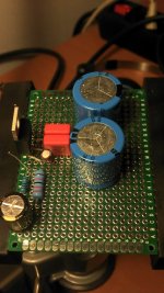
The project continues, thanks again for all the replies! Here's an illustration of the aforementioned problem:
I hadn't connected the grounds at the rectifiers. I just measured 26V between V+ and V- and assumed I was good.
After connecting the grounds I get 26V between V+/V- and GND. I was looking in the wrong places the whole time because of my lack of knowledge and experience. At least both of them went up now thanks to this. I feel so dumb though as I would probably have figured it out earlier if I hadn't just assumed the PSU was fine. Check, check and doublecheck everything the next time.Thank you @pacificblue for your reply even if it didn't solve the problem directly. It will however be useful advice in the future!
@danielwritesbac, even though I don't agree with my beautiful project being a "wiring mess" I'm considering using your guide as a reference to building my finished amp on universal board.
And @AndrewT, you said you wouldn't participate in my undertakings anymore, however I feel like you don't have the option as your great advice is imprinted all over the forums.
AndrewT said:Do not use a chassis at this first build stage.
Be very aware that without the chassis, there is nowhere to connect the Safety Earth.
No pets, no children, no nagging wife in the same room.
Build up one channel complete from input RCA to Output speaker terminals.
Find out if your single channel is hum free and buzz free. Thoroughly check it.
When you are happy that it is perfect, build up your second channel and place it alongside.
It too should be perfect.
Now couple the Main Audio Grounds on each of the two parallel assemblies.
Check for hum and buzz. Attach first one channel of source to either input. Then to the other input. Then two source channels to both inputs. Is it still completely hum free and buzz free?
When you successfully get to this two channel hum free state, you are ready to start visualising how to package the perfect amplifiers into a single chassis.
Electrically everything must remain identical.
Physically (magnetic radiation) the "in chassis assembly" will be very different. But, because the electrical side is identical, you will know that any introduced hum or buzz can only be due to magnetic radiation from and to "loops" in the circuits.
The project continues, thanks again for all the replies! Here's an illustration of the aforementioned problem:
Attachments
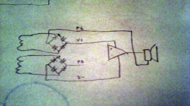
Made a preliminary layout with optional DC-blocking caps.
Signal star ground bottom left. Output with room for optional zobel up left. Power star ground between supply caps. Feedback resistor under the board for shortest possible loop.
Might be in trouble if I find that I need a lot more additional components but I'll cross that bridge when I get there.
Signal star ground bottom left. Output with room for optional zobel up left. Power star ground between supply caps. Feedback resistor under the board for shortest possible loop.
Might be in trouble if I find that I need a lot more additional components but I'll cross that bridge when I get there.
Attachments
- Status
- This old topic is closed. If you want to reopen this topic, contact a moderator using the "Report Post" button.
- Home
- Amplifiers
- Chip Amps
- Designing a LM1875-based amp