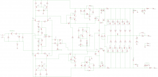
I'm still trying to find the links ....
But complimentary differential topologies are inherently unstable with
current mirrors. (too much loop gain , like "opposed" Blameless's)
Many of our old "guru's" and even Cordell have explained why.
Interesting to know, why? 🙂
Here is a model of the modified Leach Poweramp with a THD of 0,000.05% in the amplification of the signal with frequency of 20 kHz to 40 V / 8 Ohms.
Look at the R10, R11, Q22, Q21 and a current mirror with unequal resistance of resistors R5, R13. If there are problems with a positive temperature drift quiescent current Q9, Q10, it is necessary to put a diode in series with R12.
Attachments
Get rid of the input current mirrors and use matched resistors.Today I simplified the VAS as sugested. Removed Q1 and Q2 and R26, R27 Linked the base to emiters of q1 and 2 to get a simple VAS. I then removed 2nd power stage transistors Q19 and Q20 (mje15032,33) to protect output power transistors. Then removed 1 leg of R39 resistor and added a second r39 linked at a common end to create a new common point for the negative feedback wire.
Is this the usual method for removing the output stage and just testing the input, or are there other methods to do so?
Anyway, the result was a stable input stage. Voltages with a link on the input are testing the same as Ltspice is predicting with the current Circuit. What do you guys suggest as the next step now? Change the VAS to a different design again, or re install the output stage with this simple VAS installed?
Anyway, current schematic and changes are shown below.
Yeah. I really like your idea of doing that. Smart idea when doing many designs such as you like to do.
View attachment 549276
Upon checking the previous vas resistors R28,R29 they now start off at 150mv across the resistors and climb very slowly over a matter of minutes now at 260mv after around 4 minutes and continuing to rise slowly. Now sure what is causing this, maybe still oscillations but now to a lesser extent?
As some have suggested, I have tried a new VAS again, the Hawksford type. Now voltage across 10 ohm VAS resistors is 100mV (10ma). It is rock steady at that voltage. The measured DC bias measured between 0V and negative feedback point (2nd and 3rd stage power transistors not in circuit) is 0.2-0.4mV.

I will put the output stage back in circuit now.

I will put the output stage back in circuit now.
Last edited:
It's all good. What made you change circuit to control the quiescent current of Q3, Q4?As some have suggested, I have tried a new VAS again, the Hawksford type. Now voltage across 10 ohm VAS resistors is 100mV (10ma). It is rock steady at that voltage. The measured DC bias measured between 0V and negative feedback point (2nd and 3rd stage power transistors not in circuit) is 0.2-0.4mV.
Interesting to know, why? 🙂
Here is a model of the modified Leach Poweramp with a THD of 0,000.05% in the amplification of the signal with frequency of 20 kHz to 40 V / 8 Ohms.
Look at the R10, R11, Q22, Q21 and a current mirror with unequal resistance of resistors R5, R13. If there are problems with a positive temperature drift quiescent current Q9, Q10, it is necessary to put a diode in series with R12.
Hi!
attached asc file oscillates at ~150kHz...
Hi Guys
I would lose the current mirrors and keep the EF-VAS, as the latter provides an order of magnitude THD reduction.
The feedback loop is nothing that Leach used and I would change it to something more conventional. Sometimes a high-frequency oscillation is triggered by a low-frequency instability.
I would also remove the 22ks in the hum filters, if you want them just to be hum filters. If you want them to regulate, change the 22ks to zeners.
LC wrote: " I'm really getting sick viewing the same old crap in almost every new thread started"
So don't look and don't comment.
Have fun
Last edited:
Above there is such a file.Hi!
attached asc file oscillates at ~150kHz...
Hi. I haven't read everything, but I would try a few things to experiment (I'm referring to your original schematic):
- Remove T4, T7, T9, R7, R12, R13, R18 and R20, and the same on the other side
- Decrease R16 a bit, maybe 3.9k?
- Increase R6 to about 1.5k (or where you will end up with 1.5 V over it)
- Determine your amplifier stage current by setting R29 (should have about 0.3 V over it)
My reasons are that you can start simple, and work it more complex, but then you have a better understanding of the design points you wish to follow, and can calculate them easier rather than guessing. By decreasing R16, you will have 2 mA in the tail, giving 1 mA in each pair. It also gives more current to play with (you can keep your resistors a little smaller). I have found it easier working with 1 mA than 0.7 mA, and I find the extra bias helps. Then eliminating R7 and R18 will eliminate that forced local feedback (you don't really need to stabilize the emitters here - you can even use small resistors, 56 ohm or less if you really want to), giving you more open-loop gain, and thus justifying getting rid of the current mirrors. Doing all of this will make your base voltage on Q2 very predictable, which makes your voltage on R29 more predictable.
To stabilize this part of the circuit, I would try shunting C9 to the collector of Q2, rather than Q4, since Q2 and Q4 do not make a Darlington. You may even try changing Q4 for a PNP, but you will need to change the design a little here, but Q4 being a PNP will give you much better thermal stability. As an NPN, you already have at least 350 mW on it at your original design point, and I'm afraid this thing will run like the wind towards thermal breakdown, cooking Q4 and R29 in the process. You can replace it directly with the circuit shown below (NPN part), and this should give much better thermal stability, while keeping your design points and topology more or less the same. Oh, and a capacitor from base to collector on Q4 might be worth a try too, say 100 - 150 pF (circuit below already includes it).
(Replace MJE's with whatever you prefer, and heatsink them)
Also, working with small current and small resistors is quite difficult; you need to give quite a lot of tolerance. The reason is that Vbe voltages can vary tremendously from simulations to real life specs. The compound pairs shown give this tolerance, and will be happy with (I'm guessing) up to 50 mA, which is a massive tolerance.
I may be way off, but if you would like, give this a try.
- Remove T4, T7, T9, R7, R12, R13, R18 and R20, and the same on the other side
- Decrease R16 a bit, maybe 3.9k?
- Increase R6 to about 1.5k (or where you will end up with 1.5 V over it)
- Determine your amplifier stage current by setting R29 (should have about 0.3 V over it)
My reasons are that you can start simple, and work it more complex, but then you have a better understanding of the design points you wish to follow, and can calculate them easier rather than guessing. By decreasing R16, you will have 2 mA in the tail, giving 1 mA in each pair. It also gives more current to play with (you can keep your resistors a little smaller). I have found it easier working with 1 mA than 0.7 mA, and I find the extra bias helps. Then eliminating R7 and R18 will eliminate that forced local feedback (you don't really need to stabilize the emitters here - you can even use small resistors, 56 ohm or less if you really want to), giving you more open-loop gain, and thus justifying getting rid of the current mirrors. Doing all of this will make your base voltage on Q2 very predictable, which makes your voltage on R29 more predictable.
To stabilize this part of the circuit, I would try shunting C9 to the collector of Q2, rather than Q4, since Q2 and Q4 do not make a Darlington. You may even try changing Q4 for a PNP, but you will need to change the design a little here, but Q4 being a PNP will give you much better thermal stability. As an NPN, you already have at least 350 mW on it at your original design point, and I'm afraid this thing will run like the wind towards thermal breakdown, cooking Q4 and R29 in the process. You can replace it directly with the circuit shown below (NPN part), and this should give much better thermal stability, while keeping your design points and topology more or less the same. Oh, and a capacitor from base to collector on Q4 might be worth a try too, say 100 - 150 pF (circuit below already includes it).
(Replace MJE's with whatever you prefer, and heatsink them)
An externally hosted image should be here but it was not working when we last tested it.
Also, working with small current and small resistors is quite difficult; you need to give quite a lot of tolerance. The reason is that Vbe voltages can vary tremendously from simulations to real life specs. The compound pairs shown give this tolerance, and will be happy with (I'm guessing) up to 50 mA, which is a massive tolerance.
I may be way off, but if you would like, give this a try.
- Status
- Not open for further replies.
- Home
- Amplifiers
- Solid State
- Designing 200w Amplifier. Oscillations or something else? need help please.