After reading Douglas Self's book on amplifiers, I've understood there's a lot of variation and design philosophies out there.
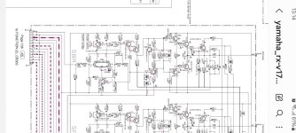
Using the schematic from my own Yamaha AVR, there are a few details I would like to understand. I can't seem to get decent results on my own searches on Google and here, and don't possess the skills to break down and analyse all sorts of circuits yet.
(1) Is there a name or explanation for the compensation scheme in this amp?
There seems to be more scattered caps plus the RC-network R304/C294, witch cap value seems very high compared to the usual Miller cap value.
(2) Q257 seems kinda like half a current mirror, or the 3rd transistor in a Wilson mirror, but without the mirror part. I haven't been able to find out exactly what is going on. I could probably do some simulations, but alas, I'm not there yet.
Attachments

Thanks for clearing that up. I've been searching for single transistor current mirror with no results, witch led me to believe there is no such thing
What about C259 and C287? Are those purely for stability?
What about C259 and C287? Are those purely for stability?
I think Q257 is a common-collector stage: the input signal is applied between its base and collector and the output signal is taken off between its emitter and collector. The advantage over an ordinary common-emitter stage is the lack of a zero in the right half plane.
@MarcelvdG - I believe you are looking at Q270.
Ed
Yes. They form a capacitive voltage divider at high frequencies.What about C259 and C287? Are those purely for stability?
Ed
A current mirror has a gain of 1. Here, Q257 has a gain of about 5, so about 83% of the output of the LTP comes from the feedback side and ~17% from the input side. Given that the current in the input side of the LTP is emitter coupled to the feedback side, it may be more accurate to say that the dominant signal path is via the inverting side of the LTP. I suspect the mindset of the time was getting the most gain possible with fewer transistors
Likewise, the mindset of the time attempted compensation with piecemeal measures. Today, if we wanted to avoid Miller caps for compensation, we would degenerate the LTP. The ~RFI cap across the LTP bases is not a great plan because it negatively impacts the feedback phase margin, vs a grounded input cap that actually improves the phase margin. These older amps were designed without the aid of simulation and the years of experience we have today. And it's possible things were done to compensate for poor ground path routing and things not illustrated by the schematic.
Likewise, the mindset of the time attempted compensation with piecemeal measures. Today, if we wanted to avoid Miller caps for compensation, we would degenerate the LTP. The ~RFI cap across the LTP bases is not a great plan because it negatively impacts the feedback phase margin, vs a grounded input cap that actually improves the phase margin. These older amps were designed without the aid of simulation and the years of experience we have today. And it's possible things were done to compensate for poor ground path routing and things not illustrated by the schematic.
@MarcelvdG - I believe you are looking at Q270.
No, I'm not. When you look at the output current of the differential pair as a floating current source, Q257 is a common-collector stage.
In fact there is a 1993 paper from Rudy Eschauzier and Johan H. Huijsing about how to avoid right half plane zeros with constructions like this. They describe it as a multipath technique, but it is simply a common-collector stage. Not grounded collector, but common collector.
https://ieeexplore.ieee.org/document/5467933?arnumber=5467933
From what year is this amplifier?
Last edited:
The ~RFI cap across the LTP bases is not a great plan because it negatively impacts the feedback phase margin, vs a grounded input cap that actually improves the phase margin.
They have both: C260 and C259. No idea why one would need both.
These older amps were designed without the aid of simulation and the years of experience we have today. And it's possible things were done to compensate for poor ground path routing and things not illustrated by the schematic.
When you still try to understand what you are doing, you are being old fashioned. Nowadays there are simulators and optimizers, so one would just draw some compensation networks here and there with parameterized values, let the optimizer dimension them and not try to understand whether the solution it comes up with makes sense. I've spent my last Christmas holiday in a team repairing the damage someone had done with that approach.
This is a new definition of "common collector". 😉MarcelvdG said:When you look at the output current of the differential pair as a floating current source, Q257 is a common-collector stage.
I figured it out.MarcelvdG said:They have both: C260 and C259. No idea why one would need both.
C260 is a conventional low-pass filter on the input.
C259 and C287 form a capacitive voltage divider that reduces the open-loop gain by 12dB at high frequencies. The -3dB point is at 78KHz. The use of a capacitive voltage divider is unusual, but it is sound engineering.
Ed
Last edited:
Common collector means that the source and load are both connected to the collector. When you look at the output of the differential pair as a floating current source, that's the case.
You could be right about C259 being for frequency compensation. The input transistors have an fT of 100 MHz at 1 mA according to https://nl.mouser.com/datasheet/2/408/HN4C06J_datasheet_en_20140301-1272629.pdf Assuming the fT at the about 0.5 mA they are biased at is between 50 MHz and 100 MHz, the capacitance between their bases (capacitance from the transistors themselves, I mean) should be somewhere between 15 pF and 30 pF. C259's value is greater than that, so at least it doesn't get swamped by the transistors themselves.
You could be right about C259 being for frequency compensation. The input transistors have an fT of 100 MHz at 1 mA according to https://nl.mouser.com/datasheet/2/408/HN4C06J_datasheet_en_20140301-1272629.pdf Assuming the fT at the about 0.5 mA they are biased at is between 50 MHz and 100 MHz, the capacitance between their bases (capacitance from the transistors themselves, I mean) should be somewhere between 15 pF and 30 pF. C259's value is greater than that, so at least it doesn't get swamped by the transistors themselves.
RX-V1700 from around 2010-2011From what year is this amplifier?
Amp is "only" 15 years old, so despite my limited knowledge I doubt a mayor player like Yamaha didn't have access to SPICE or some equivalent at the time.These older amps were designed without the aid of simulation and the years of experience we have today. And it's possible things were done to compensate for poor ground path routing and things not illustrated by the schematic.
Regarding ground path routing, that could be a possibility. Studying the service manualthere seems to have been a few iteration underway.
I really appreciate the discussion. Once more I'm duly reminded that my knowledge is extremely limited. Onwards with the reading, as it's a fascinating subject
Last edited:
- Home
- Amplifiers
- Solid State
- Design philosophies and variations in amplifiers