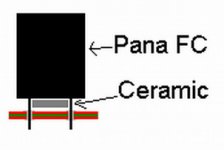
To bypass the power pins of a dac, is this an acceptable method ? You use a low value through hole electrolytic and solder a good quality smt ceramic between its pins.
It's for a ssop28 dac and space is scare. The advantages being using this combo very near of the dac, you'd be saving a lot of space (relative of course) compared to surface mounting the ceramic. Traces and DAC being on top of the board, a groundplane on the bottom.
It's for a ssop28 dac and space is scare. The advantages being using this combo very near of the dac, you'd be saving a lot of space (relative of course) compared to surface mounting the ceramic. Traces and DAC being on top of the board, a groundplane on the bottom.
Attachments
Why don't you solder the smt cap between the pins on the underside of the board? I would consider this a standard technique, as the cap will definitely fit inbetween the electrolytic's pins still on it's own pads. Thus, no tricky difference between schematic and board, no difficult work to solder the smt cap, no waste of real estate and an only insignificantly longer trace between cap and dac. Also, the now elevated electrolytic could be prone to vibration and shortened life span.

Sebastian. 😉
PS: I regularly solder smt components between tth pins.
Sebastian. 😉
PS: I regularly solder smt components between tth pins.
sek said:Why don't you solder the smt cap between the pins on the underside of the board? I would consider this a standard technique, as the cap will definitely fit inbetween the electrolytic's pins still on it's own pads. Thus, no tricky difference between schematic and board, no difficult work to solder the smt cap, no waste of real estate and an only insignificantly longer trace between cap and dac. Also, the now elevated electrolytic could be prone to vibration and shortened life span.
When making a single-sided board, I put the SMT components on top and the through-hole ones on the bottom -- you just have to remember to do all the SMT devices first.
- Status
- Not open for further replies.