I just finished my amp.
I plugged it... power... no flammes and tube being light was a good point!
But i tried to adjust bias, ok on one side but the other don't go over 280mv 🙁
And i noticed that the mosfet are not getting hot at all but the R21 resistor (big black one rated 6.5W) is hot as hell (i actually burn my finger on it).
I tried to check sound output (jack 3.5 to rca with my phone) but no sound is goind throught the speakers 🙁
any info on what could be wrong? I can post a really high res picture of the board if needed; i'm dying to ear the sound it produces!
Thanks!
It's always a good call to include pics. That way people can look for any mistakes that might have been made.
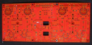
Ok, here are the two picture (220V connector) and the board+cables:
http://www.binard.biz/tmp/DSC_3240.jpg
http://www.binard.biz/tmp/DSC_3241.jpg
sorry, the files are heavy...
http://www.binard.biz/tmp/DSC_3240.jpg
http://www.binard.biz/tmp/DSC_3241.jpg
sorry, the files are heavy...
C22, C26...Do they not have polarity marking on the board or are they in backwards...I couldn't really tell.
R21 is the HV feed resistor to the screen regulator. Check your power supply section to ensure the proper voltage on the input and output of the mosfet. With the 3 50v zeners, you should have 150v on the screens. If you were to pull all 4 output tubes out, the resistor should not get hot. There are several electrolytics on this reference, be sure they are not backwards or shorted.
Check C26, I could not tell in the photo. The MosFet could be shorted to GND...
Pull the output tubes and free the Mosfet from the chassis. There is little current 2ma or so for the bleed resistors. If you have your voltages, verify no short at the MosFet mount to chassis. Or Ohm out the S and D to the chassis for low resistance-short.
Pull the output tubes and free the Mosfet from the chassis. There is little current 2ma or so for the bleed resistors. If you have your voltages, verify no short at the MosFet mount to chassis. Or Ohm out the S and D to the chassis for low resistance-short.
Attachments
Look closely at the schematic (and Pete's photos) for the output wiring - the white is the output +, the Yellow or Orange is the output - and you need to ground the output to the pcb. Just use one speaker - jack and transformer wire at this time (Yellow or Orange)
The 6.5W resistor gets hot. That's normal - it dissipates about 150v into heat.
Have you checked the voltages on the schematics? There are DC voltages printed all over it. Start at the PSU and move on from there, they all need to be verified. Fix your output wiring and then do that.
The 6.5W resistor gets hot. That's normal - it dissipates about 150v into heat.
Have you checked the voltages on the schematics? There are DC voltages printed all over it. Start at the PSU and move on from there, they all need to be verified. Fix your output wiring and then do that.
roline : the 150V shown on picture are OK. without tubes, the R21 is not getting hot. No shorts to chassis from the mosfet. I first checked the capacitor polarity, i've redone it and all seems good.
Got 350V on C17 to C20.
Got around 730V on right output plate. But left is at zero 🙁
6L6 : i tried adding the ground but i thought it was needed ony for NFB. For checking all voltage, i'll have to wait tomorrow to be able to print the schematics and check carefully step by step.
Got 350V on C17 to C20.
Got around 730V on right output plate. But left is at zero 🙁
6L6 : i tried adding the ground but i thought it was needed ony for NFB. For checking all voltage, i'll have to wait tomorrow to be able to print the schematics and check carefully step by step.
I also took a picture from the other side of the pcb if it could be helpfull : http://www.binard.biz/tmp/DSC_3268.jpg
No voltage on the plate?
If the Red transformer center tap is at B+ say 400V then the brown and blue should also be at the value if the tubes are not in. DC coupled through the transformer.
Powered up with tubes, the brown and blue primary wires should still be close to the B+ on the Red wire, low DC resistance while 6.6K dynamic AC impedance.
If the MosFets are under a lot of current do not leave them hanging without a heat sink, powering up would fry them.. very quickly.....
Judging from the jumpers you are using the cap less 6JN6 tubes??? I used the 6GV5's with the cap HV wire and ceramic cap. 6JM6 also need the cap connector.
yes it's 6JN6 tubes. I use heatsink on mosfet;
Mosfet 1, on S reads 115V and second on S it reads about 340V.
Right B+ and PLT1/2 are at around 340V and left is at 0 for all three.
Mosfet 1, on S reads 115V and second on S it reads about 340V.
Right B+ and PLT1/2 are at around 340V and left is at 0 for all three.
I one plate is at zero and you can't get a decent bais current I suspect an open circuit in the OPT or the connections to it.Got 350V on C17 to C20.
Got around 730V on right output plate. But left is at zero 🙁
The result is a far to great g2 current,bad for the tube and heating up the source of the current (resistor,mosfet).
Mona
Looks like an open trace or feed through. You will have to ohm out the B+ trace to ensure there was not a manufacturing issue with the plating or etching..
Before ohming out the B+ to the L channel plates/opt, measure the voltages in the B+ line at every point you can. At someplace you will find where it stops.
Right B+ and PLT1/2 are at around 340V and left is at 0 for all three.
Between R B+ and L B+ there are no components, only PCB trace. So if B+ is there on the L side, it should be there on the R!
The PCB manufacturer -claims- to 100% electrically test each bare board. So I am a little concerned if you really have an open trace or plated hole! 😡
With the amp powered off, and some time passage for caps to discharge, you can use an ohmmeter and put one probe on L B+ ("RED" pad). Trace it back and see where the circuit goes open: (As viewed from component side of PCB, with the text right reading) Bottom of R44, top of R49, S of Q2. I am assuming there is continuity from there on, as the S of Q2 then routes off to the left channel.
Once you find the break, carefully inspect the board and see if you can find a gap in a PCB trace along that path, or perhaps a crack next to one of the pads. Probably the most likely spot would be right at the S of Q2, on the component side...
If you did any rework (remove and replace parts) it is also possible that the hole plating got pulled out. If that's the case, once you find the open, you can simply solder the lead on both sides of the PCB and you should be OK.
Please let me know what you find!
Pete
- Status
- Not open for further replies.
- Home
- Amplifiers
- Tubes / Valves
- DCPP - "Engineer's Amplifier" : Need a bit of help