I'm going to give the Wiki system here a try. 🙂
This is a high accuracy DC servo circuit for the output stage in RocketScientist's (NwAvGuy) O2 Headphone Amplifier. The net result is a DC servo that produces a DC output correction voltage with only about 40uV (micro volts) of signal ripple given a maximum worst-case situation (for the servo circuit) input signal from the O2's output stage of 7Vpeak at 10Hz.
The circuit is essentially a repaired/improved version of the well known DC servo circuit in National Semiconductor's LME49600 Evaluation Board, here:
http://www.google.com/url?sa=t&rct=...dVjXmZiWjZxmmrrO2ZrcAIQ&bvm=bv.41524429,d.b2I (opens PDF file)
The National circuit is known to produce some variable results. Those problems are explained and fixed here.
RocketScientist's O2 Headphone Amp is here
http://www.diyaudio.com/forums/headphone-systems/193977-objective2-o2-headphone-amp-diy-project.html
The output stage consists of one dual-amplifier NJM4556 chip per channel, wired in a unity gain buffer configuration. The two sections in each chip are paralleled with 1 ohm resistors. Right off the bat, since the stage is a unity gain buffer, the DC servo will have to be an inverting circuit to be able to sum-in a negative feedback DC correction signal into the amp inputs. The original National Semiconductor DC servo circuit is non-inverting since it sums into an inverting input in that amp.
When a DC servo output is summed back into the input of an amp stage, such as in the National evaluaton board, a common misconception is that the servo is in parallel across the amp's feedback resistor. After all, that is how it appears at first glance. But the DC servo output is actually in parallel with the resistor from the amp's input to ground. The amp input can be either non-inverting or inverting, depending upon whether the servo is inverting or non-inverting, respectively.
A good way to think about this is that the output of the DC servo op amp is very low impedance, looking back into the servo op amp output, and will be at a very small DC correction voltage. So it is nearly a virtual ground. That puts the existing resistor to ground, and the new servo output resistor, essentially in parallel. The situation is easy to confirm with Spice simulations.
Fixing and Upgrading the National Semiconductor DC Servo Circuit
The Chip
The first and largest problem with National's circuit is that they used the same chip for the DC Servo as they did for the amplifier they were trying to correct the DC output on (just the other half of a dual op amp, in fact). Bad idea. The DC servo chip needs to have DC parameters much better than the chip being corrected, otherwise the best that can be hoped for is the same DC offset one started with, and likely worse, which is what often happens with the National Circuit.
DC parameters of the op amp include the input offset voltage, input bias current, input, and drift amounts for both those parameters. If the chip having its output DC offset corrected and the DC servo chip both have 3mV of worst case input DC offset, you've lost before you've begun. In this case the OPA627 and OPA211 chips are specified - either will work, although the OPA211 is SMD only - which both have input offset voltage about 1/7 of the LME49720 chip in the National circuit, worst case, and 1/60 of that in the O2's NJM4556 chips.
The OPA627 has the additional benefit of being FET input, for pico-amp input bias currents that are 1000 times smaller than the 10nA input bias currents of the bipolor LME49720, NJM4556, and OPA211.
For example, in the National evaluation circuit, the minimum datasheet input bias current for the LME49720 is 10nA, which pulls through the 1 meg ohm resistors on both the op amp inputs. That causes a voltage drop of (10nA)(1meg) = 10mV across the resistors, adding an additional 10mV of input offset to the chip's existing input offset voltage. Those two resistor IR drops will differentially sum in the op amp input and nearly cancel, however it opens the situation up to non-matching due to tolerances on the resistors and up amp input bias currents.
If one input resistor is at the low end of its 1% range at 990k and the other is at the top and at 1.001 meg, that would differentially sum to (20k)(10mA) = 400uV that would not cancel out. Input bias current differences add to that. Using the pico-amp input bias current OPA627 dramatically reduces the input resistor IR losses and hence any mismatch on differential cancellation at the op am input. It also allow larger resistors to be used. In the case of a DC servo Johnson noise levels in the large resistors don't matter since they are still below the signal levels and are dropped to vanishing small amounts by the low pass filters.
To sum it all up for the chip choice, in this instance which high levels of DC precision are needed for the DC servo, the OPA627 justifies its hefty price at $20/chip for the low grade and $30 each for the high grade. The OPA211 clocks in at $11 each with similarly low input offset voltage but bipolar inputs with the higher input bias currents.
Input Filter
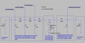
The next failing of the National evaluation DC servo is the weak input low pass filter. Looking at the schematic in the National AN-1768 application note linked above, R10 and C6 form a passive low pass filter on the non-inverting input of the servo op amp with a corner frequency of 1/(2 * Pi * 1,000,000 ohm * 0.000001F) = 0.16Hz. The goal of the LPF is to extract the DC from the input audio signal from the amplifier, of course, then feed that hopefully pure DC signal onto the integrator formed by R9 and C5.
A single stage low pass filter with Fc = 0.16 like this would work reasonably well in extracting DC at the higher end of the audio range, such as 5kHz - 20kHz. But at the very low end, 10Hz to 50Hz, things fall apart badly. A single stage LPF just can't get the AC components down enough to prevent signal AC, along with the DC servo correction voltage, from being fed back into the amp input. This means that in additon to being a DC servo, at the lower end of the audio frequency spectrum the circuit is inadvertantly acting as a global AC feedback loop, and AC rather out of phase at that. Not a desired result in a DC servo.
The solution is to casacade more passive RC filter stages together to truely extract pure DC at 10Hz before feeding it on into the integrator. As for why I'm specifiying 10Hz, from past email with RocketScientist he preferred to test his systems down to 10Hz for some reason. Since its his amp, and he clearly knew more about this stuff than me, I'm running with that. 🙂
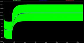
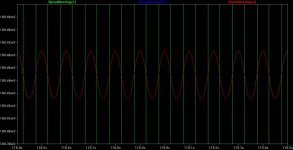
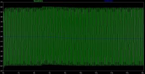
As for what constitutes "pure DC" out of the low pass filter, there will be AC ripply on the output of any LPF. It just comes down to what is acceptable. In this case the worst-case input offset voltage of the OPA627 is 100uV, so I'm specifying that the maximum ripple on the DC extracted by the LPF should be less than that. 3 passive stages with Fc = 0.16Hz for each result in 40uV of ripple, as shown in the LT Spice plots below, with the O2's maximum 7Vpeak output swing at 10Hz. Two stages, as shown in the plots, only achieved 1.5mVpeak.
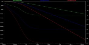
And the single stage RC LPF in National's orignal circuit, as shown on the right half of that LT Spice test plot, is equal to one stage here (this circuit and theirs have Fc = 0.16Hz per stage), at 180mVpeak.
The AC plots below tell the story. At 10Hz a single stage in either the original filter or this one is down about 36dB (green in the plot). The second stage is down about 73dB (blue) at 10Hz while the third stage is down 111dB.
In the transient plot below the voltage sources are in the middle. One is 7Vpeak at 10Hz for the maximum O2 output at the lowest frequency. The other is a pulse source simulating the DC offset fault at 200mV which kicks in at 15 seconds. The three filters to the right of the sources are this circuit, while the one stage to the right is National's original input circuit. Since both National's circuit and the first stage here have FC = 0.16, the plots lay right on top of each other with minor phase differences. For that reason I've omitted National's on the AC plot for clarity.
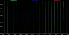
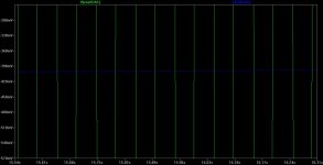
The first two transient plots show all 3 filter stage outputs. The next zooms in on the 2nd stage output (blue) while the last zooms in on the 2rd stage output (red) showing about 40uV of the 10Hz left - "pure DC" for our purposes here vs. the input offset voltage of the OPA627.
Integrator Circuit
The integrator in National's circuit is formed by R9, C5, and the op amp. The output of the integrator goes through R5 which is in parallel with R1 as discussed above, NOT in parallel with the feedback resistor R3. The parallel combo of R5 and R1 produce 500 ohms, which gives the amplifier circuit a gain of (1 + (1k [R3] / 500 ohms)) = 2.
Their integrator works very simply by mathematically integrating any DC voltage at the non-inverting input, which results in an output of a diagonal line from a small DC voltage on up to the maximum rail voltage of the op amp, about 10Vdc for +/-12Vdc rails. A negative voltage going in would integrate down to the negative rail, of course. Where things get a bit mucked up is that any AC ripple on that DC going in will also get integrated. Recall that the integral of a sin is a cosine, so sinusoidal ripple on the DC going in winds up as sinusoidal ripple on that diagonal DC voltage out of the integrator heading up to the rails. That AC then gets summed right into the input of the amplifer, along with the DC offset correction voltage, forming another AC global feedback loop. Hence the importance of keeping the input DC relatively pure with the multistage low pass filter.
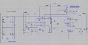
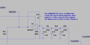
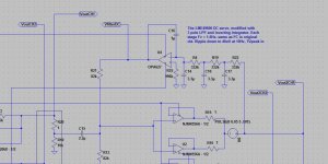
In our case we need an inverting integrator since the O2's output stage is non-inverting. The next circuit diagram below shows the new inverting DC servo setup with the 3 stage input LPF. The servo RC parameters are the same as in the National circuit - they just affect the rate of integration (slope of the diagonal DC line on the integrator output), with the exception of the 1 meg resistor being moved to the non-inverting input so the IR drop formed by the input bias current will equal and differentially cancel with the IR drop across the 3 summed 332K = 996K filter resistors.
Mouser has 332k resistors in 0.1% tolerance in both through hole and SMD but they don't have 1 meg resistors or 996K in 0.1%. They do have 449K in 0.1%, so two of those can be put in series to form the 996K (998K actually). ).1% resistor don't cost substantially more than the 1% and are important here to keep the IR drops caused by the op amp input bias current equal on both inputs. The capacitor tolerances are less critical, as are the types since the output here is just DC and not part of the AC signal path. Mouser as poly film 3.3uF caps at 63Vdc in 5% and 10% in through hole. They have MLCC ceramics in 10% in both through hole and SMD. Again, the voltage dependent capacitance change in the ceramic is less of an issue here since the output is just DC. The 5% film is probably the preferred cap is cost isn't a big issue (about $3 each).
Adding the DC Servo Into The O2 Headphone Amp
The schematic below also shows how the new DC servo hooks into the O2. The servo input comes from the O2 output jack, or from connector J2 that goes to the output jack. Rocket Scientist used a 40.2K resistor to supply the input bias current to each NJM4556 chip, R12 and R13. As per the discussion above the DC servo output will be in parallel with those resistors, so to maintain the same resistance to ground they need to be increased to 82K and an 82K resistor will be used from the servo output. The two 82Ks in parallel give 41K, of course.
However, if desired, an O2 improvement modification could be made here. R12 and R13 form low pass filters with C13 and C14 with an Fc of about 10Hz as I recall. In the modification thread I went through the details of how increasing the two film caps to 4.7uF would drop that Fc slightly, although probably not audibly. The same goes for these two resistors. Doubling RocketScientist's orignal 40.2K value to 82K would also drop the O2's low frequency Fc by a similar amount, but at the expense of double the output DC offset portion caused by the NJM4556 input bias current. Well, we are adding a DC servo, so that doesn't matter anymore! The additional offset voltage is well within the correction range of this servo. So R12 and R13 could actually be increased to 160K, and the servo output resistor increased to 160K, for the low frequency Fc improvement modification. This could be in conjunction with the mod to increase the caps to 4.7uF for a 4x drop in the O2's low frequency cutoff response.
The DC servo circuit has enough parts that it really requires a separate PC board. The simplest thing would be to use the taller B3-080 chasis and slide the board in upside down in the case's top slot, above the O2 PCB. Then the output signal, servo output, and power/ground from the mosfets can be easily cabled over to the new servo board. I'm working on a PCB layout, that probably won't be don't anytime soon, lol. Anyone wishing to lay one out could do it either through hole or SMD since the OPA627 comes in both packages.
One note on the chip. Don't use the high open loop gain OPA637. The chip requires a minimum gain of 5x which the servo won't have at high (noise) frequencies due to the integrator feedback cap. Also don't use input protection diodes as I inadvertantly showed in the mod thread for the e-12 booster circuit. 1N4148s have about 45nA of reverse current, thousands of times more than the OPA627 FET input. The datasheet shows how diode connected FETs could be used for about 1nA of current, but those are not needed here. The OPA627 inputs are protected to +Vs+2Vdc and -V-2Vdc, neither of which can be exceeded here.
Click on any of the plots below, once opened, to increase the plot's resolution.
The final two plots below show the results with the DC servo circuit added to the O2. The input voltage source to the top channel on the schematic is set at 2.5Vac at 10Hz. The gain of the stage is 2.5, so that is a total output voltage (green on the plots) of 2.5 x 2.5 = 6.25Vdc. I set that slightly below the 7Vdc max of O2 to avoid simulation problems with the device models and to leave room for the injected DC offset pulse. That DC fault pulse voltage source is added at the output of the top channel on the schematic. +200mV at the 5 second point.
The last plot shows the final result, the output of the DC servo: -400mV, which is exactly the right number after it goes through the 82k/82K 50%/50% voltage divider to ground, yeilding -200mV at the NJM4556 inputs, which exactly cancels the +200mV DC fault at the output. Q.E.D.. 😀
This is a high accuracy DC servo circuit for the output stage in RocketScientist's (NwAvGuy) O2 Headphone Amplifier. The net result is a DC servo that produces a DC output correction voltage with only about 40uV (micro volts) of signal ripple given a maximum worst-case situation (for the servo circuit) input signal from the O2's output stage of 7Vpeak at 10Hz.
The circuit is essentially a repaired/improved version of the well known DC servo circuit in National Semiconductor's LME49600 Evaluation Board, here:
http://www.google.com/url?sa=t&rct=...dVjXmZiWjZxmmrrO2ZrcAIQ&bvm=bv.41524429,d.b2I (opens PDF file)
The National circuit is known to produce some variable results. Those problems are explained and fixed here.
RocketScientist's O2 Headphone Amp is here
http://www.diyaudio.com/forums/headphone-systems/193977-objective2-o2-headphone-amp-diy-project.html
The output stage consists of one dual-amplifier NJM4556 chip per channel, wired in a unity gain buffer configuration. The two sections in each chip are paralleled with 1 ohm resistors. Right off the bat, since the stage is a unity gain buffer, the DC servo will have to be an inverting circuit to be able to sum-in a negative feedback DC correction signal into the amp inputs. The original National Semiconductor DC servo circuit is non-inverting since it sums into an inverting input in that amp.
When a DC servo output is summed back into the input of an amp stage, such as in the National evaluaton board, a common misconception is that the servo is in parallel across the amp's feedback resistor. After all, that is how it appears at first glance. But the DC servo output is actually in parallel with the resistor from the amp's input to ground. The amp input can be either non-inverting or inverting, depending upon whether the servo is inverting or non-inverting, respectively.
A good way to think about this is that the output of the DC servo op amp is very low impedance, looking back into the servo op amp output, and will be at a very small DC correction voltage. So it is nearly a virtual ground. That puts the existing resistor to ground, and the new servo output resistor, essentially in parallel. The situation is easy to confirm with Spice simulations.
Fixing and Upgrading the National Semiconductor DC Servo Circuit
The Chip
The first and largest problem with National's circuit is that they used the same chip for the DC Servo as they did for the amplifier they were trying to correct the DC output on (just the other half of a dual op amp, in fact). Bad idea. The DC servo chip needs to have DC parameters much better than the chip being corrected, otherwise the best that can be hoped for is the same DC offset one started with, and likely worse, which is what often happens with the National Circuit.
DC parameters of the op amp include the input offset voltage, input bias current, input, and drift amounts for both those parameters. If the chip having its output DC offset corrected and the DC servo chip both have 3mV of worst case input DC offset, you've lost before you've begun. In this case the OPA627 and OPA211 chips are specified - either will work, although the OPA211 is SMD only - which both have input offset voltage about 1/7 of the LME49720 chip in the National circuit, worst case, and 1/60 of that in the O2's NJM4556 chips.
The OPA627 has the additional benefit of being FET input, for pico-amp input bias currents that are 1000 times smaller than the 10nA input bias currents of the bipolor LME49720, NJM4556, and OPA211.
For example, in the National evaluation circuit, the minimum datasheet input bias current for the LME49720 is 10nA, which pulls through the 1 meg ohm resistors on both the op amp inputs. That causes a voltage drop of (10nA)(1meg) = 10mV across the resistors, adding an additional 10mV of input offset to the chip's existing input offset voltage. Those two resistor IR drops will differentially sum in the op amp input and nearly cancel, however it opens the situation up to non-matching due to tolerances on the resistors and up amp input bias currents.
If one input resistor is at the low end of its 1% range at 990k and the other is at the top and at 1.001 meg, that would differentially sum to (20k)(10mA) = 400uV that would not cancel out. Input bias current differences add to that. Using the pico-amp input bias current OPA627 dramatically reduces the input resistor IR losses and hence any mismatch on differential cancellation at the op am input. It also allow larger resistors to be used. In the case of a DC servo Johnson noise levels in the large resistors don't matter since they are still below the signal levels and are dropped to vanishing small amounts by the low pass filters.
To sum it all up for the chip choice, in this instance which high levels of DC precision are needed for the DC servo, the OPA627 justifies its hefty price at $20/chip for the low grade and $30 each for the high grade. The OPA211 clocks in at $11 each with similarly low input offset voltage but bipolar inputs with the higher input bias currents.
Input Filter
The next failing of the National evaluation DC servo is the weak input low pass filter. Looking at the schematic in the National AN-1768 application note linked above, R10 and C6 form a passive low pass filter on the non-inverting input of the servo op amp with a corner frequency of 1/(2 * Pi * 1,000,000 ohm * 0.000001F) = 0.16Hz. The goal of the LPF is to extract the DC from the input audio signal from the amplifier, of course, then feed that hopefully pure DC signal onto the integrator formed by R9 and C5.
A single stage low pass filter with Fc = 0.16 like this would work reasonably well in extracting DC at the higher end of the audio range, such as 5kHz - 20kHz. But at the very low end, 10Hz to 50Hz, things fall apart badly. A single stage LPF just can't get the AC components down enough to prevent signal AC, along with the DC servo correction voltage, from being fed back into the amp input. This means that in additon to being a DC servo, at the lower end of the audio frequency spectrum the circuit is inadvertantly acting as a global AC feedback loop, and AC rather out of phase at that. Not a desired result in a DC servo.
The solution is to casacade more passive RC filter stages together to truely extract pure DC at 10Hz before feeding it on into the integrator. As for why I'm specifiying 10Hz, from past email with RocketScientist he preferred to test his systems down to 10Hz for some reason. Since its his amp, and he clearly knew more about this stuff than me, I'm running with that. 🙂
As for what constitutes "pure DC" out of the low pass filter, there will be AC ripply on the output of any LPF. It just comes down to what is acceptable. In this case the worst-case input offset voltage of the OPA627 is 100uV, so I'm specifying that the maximum ripple on the DC extracted by the LPF should be less than that. 3 passive stages with Fc = 0.16Hz for each result in 40uV of ripple, as shown in the LT Spice plots below, with the O2's maximum 7Vpeak output swing at 10Hz. Two stages, as shown in the plots, only achieved 1.5mVpeak.
And the single stage RC LPF in National's orignal circuit, as shown on the right half of that LT Spice test plot, is equal to one stage here (this circuit and theirs have Fc = 0.16Hz per stage), at 180mVpeak.
The AC plots below tell the story. At 10Hz a single stage in either the original filter or this one is down about 36dB (green in the plot). The second stage is down about 73dB (blue) at 10Hz while the third stage is down 111dB.
In the transient plot below the voltage sources are in the middle. One is 7Vpeak at 10Hz for the maximum O2 output at the lowest frequency. The other is a pulse source simulating the DC offset fault at 200mV which kicks in at 15 seconds. The three filters to the right of the sources are this circuit, while the one stage to the right is National's original input circuit. Since both National's circuit and the first stage here have FC = 0.16, the plots lay right on top of each other with minor phase differences. For that reason I've omitted National's on the AC plot for clarity.
The first two transient plots show all 3 filter stage outputs. The next zooms in on the 2nd stage output (blue) while the last zooms in on the 2rd stage output (red) showing about 40uV of the 10Hz left - "pure DC" for our purposes here vs. the input offset voltage of the OPA627.
Integrator Circuit
The integrator in National's circuit is formed by R9, C5, and the op amp. The output of the integrator goes through R5 which is in parallel with R1 as discussed above, NOT in parallel with the feedback resistor R3. The parallel combo of R5 and R1 produce 500 ohms, which gives the amplifier circuit a gain of (1 + (1k [R3] / 500 ohms)) = 2.
Their integrator works very simply by mathematically integrating any DC voltage at the non-inverting input, which results in an output of a diagonal line from a small DC voltage on up to the maximum rail voltage of the op amp, about 10Vdc for +/-12Vdc rails. A negative voltage going in would integrate down to the negative rail, of course. Where things get a bit mucked up is that any AC ripple on that DC going in will also get integrated. Recall that the integral of a sin is a cosine, so sinusoidal ripple on the DC going in winds up as sinusoidal ripple on that diagonal DC voltage out of the integrator heading up to the rails. That AC then gets summed right into the input of the amplifer, along with the DC offset correction voltage, forming another AC global feedback loop. Hence the importance of keeping the input DC relatively pure with the multistage low pass filter.
In our case we need an inverting integrator since the O2's output stage is non-inverting. The next circuit diagram below shows the new inverting DC servo setup with the 3 stage input LPF. The servo RC parameters are the same as in the National circuit - they just affect the rate of integration (slope of the diagonal DC line on the integrator output), with the exception of the 1 meg resistor being moved to the non-inverting input so the IR drop formed by the input bias current will equal and differentially cancel with the IR drop across the 3 summed 332K = 996K filter resistors.
Mouser has 332k resistors in 0.1% tolerance in both through hole and SMD but they don't have 1 meg resistors or 996K in 0.1%. They do have 449K in 0.1%, so two of those can be put in series to form the 996K (998K actually). ).1% resistor don't cost substantially more than the 1% and are important here to keep the IR drops caused by the op amp input bias current equal on both inputs. The capacitor tolerances are less critical, as are the types since the output here is just DC and not part of the AC signal path. Mouser as poly film 3.3uF caps at 63Vdc in 5% and 10% in through hole. They have MLCC ceramics in 10% in both through hole and SMD. Again, the voltage dependent capacitance change in the ceramic is less of an issue here since the output is just DC. The 5% film is probably the preferred cap is cost isn't a big issue (about $3 each).
Adding the DC Servo Into The O2 Headphone Amp
The schematic below also shows how the new DC servo hooks into the O2. The servo input comes from the O2 output jack, or from connector J2 that goes to the output jack. Rocket Scientist used a 40.2K resistor to supply the input bias current to each NJM4556 chip, R12 and R13. As per the discussion above the DC servo output will be in parallel with those resistors, so to maintain the same resistance to ground they need to be increased to 82K and an 82K resistor will be used from the servo output. The two 82Ks in parallel give 41K, of course.
However, if desired, an O2 improvement modification could be made here. R12 and R13 form low pass filters with C13 and C14 with an Fc of about 10Hz as I recall. In the modification thread I went through the details of how increasing the two film caps to 4.7uF would drop that Fc slightly, although probably not audibly. The same goes for these two resistors. Doubling RocketScientist's orignal 40.2K value to 82K would also drop the O2's low frequency Fc by a similar amount, but at the expense of double the output DC offset portion caused by the NJM4556 input bias current. Well, we are adding a DC servo, so that doesn't matter anymore! The additional offset voltage is well within the correction range of this servo. So R12 and R13 could actually be increased to 160K, and the servo output resistor increased to 160K, for the low frequency Fc improvement modification. This could be in conjunction with the mod to increase the caps to 4.7uF for a 4x drop in the O2's low frequency cutoff response.
The DC servo circuit has enough parts that it really requires a separate PC board. The simplest thing would be to use the taller B3-080 chasis and slide the board in upside down in the case's top slot, above the O2 PCB. Then the output signal, servo output, and power/ground from the mosfets can be easily cabled over to the new servo board. I'm working on a PCB layout, that probably won't be don't anytime soon, lol. Anyone wishing to lay one out could do it either through hole or SMD since the OPA627 comes in both packages.
One note on the chip. Don't use the high open loop gain OPA637. The chip requires a minimum gain of 5x which the servo won't have at high (noise) frequencies due to the integrator feedback cap. Also don't use input protection diodes as I inadvertantly showed in the mod thread for the e-12 booster circuit. 1N4148s have about 45nA of reverse current, thousands of times more than the OPA627 FET input. The datasheet shows how diode connected FETs could be used for about 1nA of current, but those are not needed here. The OPA627 inputs are protected to +Vs+2Vdc and -V-2Vdc, neither of which can be exceeded here.
Click on any of the plots below, once opened, to increase the plot's resolution.
The final two plots below show the results with the DC servo circuit added to the O2. The input voltage source to the top channel on the schematic is set at 2.5Vac at 10Hz. The gain of the stage is 2.5, so that is a total output voltage (green on the plots) of 2.5 x 2.5 = 6.25Vdc. I set that slightly below the 7Vdc max of O2 to avoid simulation problems with the device models and to leave room for the injected DC offset pulse. That DC fault pulse voltage source is added at the output of the top channel on the schematic. +200mV at the 5 second point.
The last plot shows the final result, the output of the DC servo: -400mV, which is exactly the right number after it goes through the 82k/82K 50%/50% voltage divider to ground, yeilding -200mV at the NJM4556 inputs, which exactly cancels the +200mV DC fault at the output. Q.E.D.. 😀
Attachments
-
 DC Servo Low Pass Filter Test Circuit.jpg165.1 KB · Views: 467
 -
 DC Servo Low Pass Filter Test Circuit AC plot.jpg48.6 KB · Views: 324
 -
 DC Servo Low Pass Filter Test Circuit transient plot 1.jpg43 KB · Views: 314
 -
 DC Servo Low Pass Filter Test Circuit transient plot 2.jpg66 KB · Views: 273
 -
 DC Servo Low Pass Filter Test Circuit transient plot 3.jpg70.4 KB · Views: 281
 -
 DC Servo with LPF and integrator in O2.jpg169.6 KB · Views: 390
 -
 DC Servo - LPF + Integrator zoomed.jpg111 KB · Views: 299
 -
 DC Servo - LPF + Integrator zoomed 2.jpg93.2 KB · Views: 304
 -
 DC Servo with LPF and integrator in O2 2.5V input 2.5x gain 0.2 offset at 5sec 1.jpg170.4 KB · Views: 208
 -
 DC Servo with LPF and integrator in O2 2.5V input 2.5x gain 0.2 offset at 5sec 2.jpg51.4 KB · Views: 158