Hi,
i have build two Amps with a Connex 500R/+-45 Volt SMPS and FH9 XRK Mod boards.
The Amps are working without any problems, but the offset is rather high on all boards. Two boards get an offset of 19/21 mV the other two boards get 26 and 29 mV.
What have i done before...
Tried to measure VGS of the Mosfet belonging to the schematic of Mr. N. Pass. Got luck i could find enough matching pairs for example 4,00 volts VGS for one pair IRFP240/IRFP9240 for a board. The other pairs are not very VGS different, say 4,02 and 4,04 volts VGS or similar.
Took T6 MPSA92 out and choose a 2N5401 as replacement. The 2N5401 has a litle bit higher hFE.
Soldered out the KSC 1845 and matched every pair with my Peak Atlas, without heat and with heating. Finding matched pairs and put them in. For example hFE 420 and Vbe 727.
Nothing helps..the offset remains at high 26 mV.
Changed the KSC1845 to 2SC2240, yeah...50 mV offset...ok, seems not to be the right way....
The mosfet drivers are matched Toshiba TTC004B/TTA004B instead of KSC1381/KSC3503
If i measure PIN 1 to ground at IRFP's i got different voltages. 3,96 volts at the IRFP 240 and 3,74 volts at the IRFP 9240.
Chris, Cherman, gave me an advice to change the gate resistor at IRFP 240 from 220 Ohm to 330 Ohm as a try. Done without success.
If i do that and change the gate stopper both IRFP have less voltages in the same proportion. 3,92 volt/3,68 volt
Another idea was to change the resistor R15 at the driver to the N channel from 47 to 56 ohm or more....nothing...no success
Surely i have controlled every component, resistors, diodes..and so on...
Amp is stable with its offset about 20 mV or a liitle bit higher, no problem to adjust the bias. I choosed 120 mA, 26,4 mV over the 0,22 ohm resistor.
Has anyone an idea what else i can do to lower the offset ? Any idea to make something better is welcome.
Many thanks to Chris, cherman, helping as far he could ...
Greets
Peter
Attachments

![IMG_20250214_183418[1].jpg](/community/data/attachments/1329/1329954-21ff6c243109ce8e9d942e3fe90788bf.jpg?hash=mhaiQ_--Qf)
Hi Peter.
I am not the expert but the transconductance of PCH is typical 4.2 and NCH ist about 6.9.
So it ist needed to give the pch mosfet a bit more voltage and or give the nch less voltage. So the source resistor must be a bit bigger at the NCH mosfet.
So add a 0.01 Ohm resistor to the source resistor of the NCh.
Or
Measure both Rs. The 3 or 5 Watt resistor have tolerances so use the bigger resistor at the NCh
Kr Chris

Ok, i will try to give the Nchannel a bit less voltage..about 56 Ohm and the pchannel 39 ohm ( to use the usual resistors ) at the drivers.
The gate stopper on N channel i will change to 330 ohm.
You mean 0,1 Ohm, not 0,01 ? Why at the Nchannel ? 0,1 Ohm at the Pchannel right ?
I use Vishay and IOR Mosfets, some bought at Mouser others at german companys.. a few i have measured yesterday, ordered at Mouser. All about 4,59 VGS for the N channel. To high for my p channel mosfets...but i think the values are normal.
The Peak Atlas is not able to measure VGS correctly. Therefore i build a little board, see pdf.
I had tried my little heatings, ordered az AE. They take about 300 mA at 12 Volt first, reaching temperature of 40 grad celsius only 160 mA. Rising is much slow, i dont need a timer...dont believe they reach 50 grad.
Thank you Chris
Attachments
The output error voltages you report seem reasonable, and offset less than 100mV is typically deemed acceptable. But if you wish, you may be able to reduce the offset error.
Because the early stages of the amp produce large open-loop gain, it’s unlikely you will observe any effect from efforts to adjust matching of the output transistors. Rather, the offset likely originates at the input stage.
You mention output voltages of about 20mV and almost 30mV. Are they positive, or might they negative with respect to ground?
Would you report voltage drops across R12 and R13?
Would you also report voltages at amp output, base of T1, and base of T2? Please indicate negative voltages as signed numbers.
Thanks.
I have done all changes of advices....nope. Now i get -33 mV offset...that seems not to be the way...
I will change back exept the 47 Ohm MPR 0,1 %.
I will report....
@BSST
I report the voltages at R12/R13 and base voltage of T1/T2
Greets
Peter
I will change back exept the 47 Ohm MPR 0,1 %.
I will report....
@BSST
I report the voltages at R12/R13 and base voltage of T1/T2
Greets
Peter
Forgotten to mention....
Before the last changes the DC offset on all 4 boards were positiv measured to ground.
I know i could live with about 26mV offset. I wonder what could be the reason...all my other amps have an lower offset. To less knowledge...but perhaps i can learn something...🙂
Greets
Peter
Before the last changes the DC offset on all 4 boards were positiv measured to ground.
I know i could live with about 26mV offset. I wonder what could be the reason...all my other amps have an lower offset. To less knowledge...but perhaps i can learn something...🙂
Greets
Peter
Hi...
@ de Ocampo
Not until now. In the moment all changes set back to the values seen in the schematic. Ii have recognized that XRK has diiferent values in his amp, but for the input not for T6, MPSA92. R12/13 1k instead of 680 ohm , R6 from 270 ohm to 220 ohm.
I think it could be a input problem with the high offset. As i changed KSC1845 to 2SC2240 the output was about 50 mv. It seems that changes in the amp input take influence to the output..at every amp will be the same.
What do you think about the values of R7/R14. For testing i can change...
Greets
Peter
Please read what BSST write carefully.
Offset is a d.c voltage haven to do with input matching,not the output!
20mV offset is a very good value for a no servo amplifier.
Offset is a d.c voltage haven to do with input matching,not the output!
20mV offset is a very good value for a no servo amplifier.
Hi thimios,
as i wrote..i can live with 20 mV, but would like a little lower offset.
I want to understand what i can do to make the offset more less. In Prasi's schematic is an advice to match T1/T2.
I have done the matching as good as i can, spending hours with about hundret of KSC1845.
Then matching IRFP's and got matched Toshiba drivers. Prasi wrote about 0-10mv offset..öhh..far away with my boards.
Ok, i can order MPR resistors with only 0,1 %. I think i will order all resistors at the input new in 0,1 %.
Tomorrow or in the next days i will controll the bias of the board, done the changes before, because i had only two 47 ohm resistors 0,1 % in stock, perhaps little success...i will see
Peter
I predict that you will find voltage drop across R13 is much smaller than drop across R12. If so, that's an indication that T2 collector current is not well matched to T1 current. Try installing a jumper wire across D7, so that D7 is effectively removed from the circuit. Check if you find improvement.
Since you have already matched the input pair, and I've read swapping devices also did not work out, it seems the other option to do is to change values of the resistors in the input stage and since T6 base is tied to the collector of T2 it also influences the current flow. You may try adjusting the values of R7/R14. This is a compact circuit with only few components, it is very sensitive to changes. I have been playing with this circuit in simulation a year ago. 🙂Hi...
@ de Ocampo
What do you think about the values of R7/R14. For testing i can change...
Greets
Peter
Albert
I also noticed that you have lifted ground (RG 10R resistor) used for the input stage, but at the same time you have
R5 (2k2) from the T7 CCS connected to it. R5 should be connected to the dirty (output) ground.
Assuming there is 2mA flowing through R5 (and in consequence through RG), it will generate exactly 20mV offset on RG.
10Ohm * 2mA = 20mV.
Try connecting R5 to the dirty ground, and see if output offset is gone.
Alternatively, you can try to measure output DC offset vs clean input ground, and see if you are getting lower number.
If you do, then I'm right.
Another alternative - short RG, and verify DC offset.
Last edited:
Aha too...🙂
@minek123
Then the second schematic makes sense. I did not know why different schematics are existing and why the gerber files gave the board i used, alonging to the first schematic. I think Chris, Chermann, is using the same board.
I will try to short RG first. If i get hum, i will use the dirty ground with R5, 22k. A short wire to ground at RG seems possible with not much crossings.
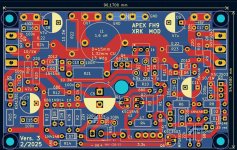
I have designed a new pcb with schematic number 2. The feedback capacitor will be bigger, 12,5 mm to fit Muse NP.
Thanks a lot...
Peter
@minek123
Then the second schematic makes sense. I did not know why different schematics are existing and why the gerber files gave the board i used, alonging to the first schematic. I think Chris, Chermann, is using the same board.
I will try to short RG first. If i get hum, i will use the dirty ground with R5, 22k. A short wire to ground at RG seems possible with not much crossings.
I have designed a new pcb with schematic number 2. The feedback capacitor will be bigger, 12,5 mm to fit Muse NP.
Thanks a lot...
Peter
Attachments

- Home
- Amplifiers
- Solid State
- DC Offset too high at my FH9 XRK Mod