Hi everyone,
I'm repairing an outlaw 7125. This amplifier is an AB class with only one potentiometer to adjust bias. Nothing to adjust dc offset.
Anyway i have 7v and 3v on 2 channel. Do you know what is causing this ? I'm comparing a working and a bad channel and i found nothing. Already replace all capacitors. Test every transistors and resistors. I'm not able to find the source of this issue.
I tried to have the schematic or service manual but it's not available anywhere. I wrote to company and not providing any schematic.
So i did it. But again i dont find the problem. I will need help on this one.
I read somewhere that some model without dc offset adjustment, transistor need to be matched. Is it possible ti have good transistor but not matching anymore ?
This is my schematic:
Microsoft OneDrive - Access files anywhere. Create docs with free Office Online.
Thank you for your help.
Last edited:
The circuit has unity gain at DC (see R43, R44, C10), so it doesn't need an output zero adjust.
Suggest you measure, and compare between channels, the DC voltages at all circuit nodes.
Suggest you measure, and compare between channels, the DC voltages at all circuit nodes.
Last edited:
Check the schematic for errors in Q3,4,5,6,8.9.10 & 11. And update the schematic.
Duke
Hi Duke, you dont trust my skill ? 🙂 Seriously, i double check this morning those transistors. And i didn't fine any errors. I know this strange arrangement, some transistor base tie to rail by resistors but the circuit is like that.
I update the schematic by moving transistor face to face, more easy to follow but wire is all in same place.
@rayma
So you are telling me that is suppose to have a dc feedback to correct the output. Coming from tension divider r9-r10 to r44. Charging c10 by r43 ?
If so, something is wrong with this but what exactly... 😕
Channel image for reference
An externally hosted image should be here but it was not working when we last tested it.
Microsoft OneDrive - Access files anywhere. Create docs with free Office Online.
Thank you
Last edited:
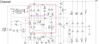
Your schematic VAS stage Q6 and C6 connection seems not correct, I just point out in small circles for the positive rail one side only, please double check their correct circuit connection and the Q10/Q11 base pins also.
Best regards,
Patrick
Thank you to have take the time. I'll double check again. I'll be back to you soon.
The input stage differential pair transistors Q1/Q2 and the voltage amplifier stage Q8 to Q11 transistors can cause the DC output offset.
For these small signal transistors, we can simple use a multimeter built-in Hfe testing function to measure their Hfe and match them with the closed Hfe value, it is the same way to match NPN to PNP transistors.
In your case, please try test or replace the voltage amplifier stage Q8 to Q11 transistors first, if no result then test the differential pair transistors.
@Patrick and Audio1man, you were right, i did a mistake. And Patrick, you point out exactly my mistake. I updated the schematic now. thank you.
For the transistor q1,q2 and q8-q11 i have good news. This is the hfe:
Q8 = 96
Q9= 93
Q10 = 196
Q11 = 165
Q1 A =396
Q1 B = 395
Q2 A = 534
Q2 B = 26
Why the problem is always the last one unsoldered ? 😀
So it's clear to me that Q2 B is defective. Good in diode tester but bad. It's a 2sc3200 and availability doesn't look good. digikey 0, mouser 0. Available on ebay but i'll wait 2 months. Maybe you know good substitute ?
2SC3200 datasheet
Also Q10 and Q11 are not matched perfectly, i dont know if this can be a problem. I dont have very large experience with this. What do you think ?
Thank you again.
Why the problem is always the last one unsoldered ? 😀
Murphy's law?🙂
Maybe you know good substitute?
KSA992FTA/KCS1845FTA from Mouser...take a minimum of 20 pieces each to find a good pair of each sex, pair them to Vbe and Hfe.
SA992FTA/KCS1845FTA from Mouser...take a minimum of 20 pieces each to find a good pair of each sex, pair them to Vbe and Hfe.
You are saying i must replace all 4 (2 npn/2 pnp) ?
Is the hfe/Vbe of npn must match pnp too ?
Is the fact of iC SA992FTA/KCS1845FTA is 50 ma instead 100 ma is ok ?
And for Q10 = 196 Q11 = 165 is them ok ?
I know a lots of questions 🙂 Thank you!
For the transistor q1,q2 and q8-q11 i have good news. This is the hfe:
Q8 = 96
Q9= 93
Q10 = 196
Q11 = 165
Q1 A =396
Q1 B = 395
Q2 A = 534
Q2 B = 26
Why the problem is always the last one unsoldered ? 😀
So it's clear to me that Q2 B is defective. Good in diode tester but bad. It's a 2sc3200 and availability doesn't look good. digikey 0, mouser 0. Available on ebay but i'll wait 2 months. Maybe you know good substitute ?
Also Q10 and Q11 are not matched perfectly, i dont know if this can be a problem.
It is due to a 7-Channel Amplifier, if you change the input pair transistors, please consider to change at least two amp of the same kind channel for a balance of that channel.
The input transistors you can use 2SC2240/2SA970(if you can buy), or KSA992FTA/KCS1845FTA will be ok.
For the VAS transistors, you can try to replace with better matched transistors if the output DC offset is not good.
Last edited:
You are saying i must replace all 4 (2 npn/2 pnp) ?
Is the hfe/Vbe of npn must match pnp too ?
Is the fact of iC SA992FTA/KCS1845FTA is 50 ma instead 100 ma is ok ?
And for Q10 = 196 Q11 = 165 is them ok ?
For input transistors maximum collector current is not so important, it will not run very large current, but the maximum collector emitter voltage is more important.
Better change four input transistors with matched pair of npn to pnp.
For VAS, you check the DC output offset first and then can decide change or not.
Q1) In fact yes, if you only change the Q2B the amplifier will start working, but on the output it will have a DC offset again, as Murphy says. If you change and pair only the Q2A / Q2B the amplifier will work normally, but again with some DC offsets on the output, probably acceptable for normal operation. If you change and pair all transistors at the input differentials, the amplifier will operate at min. DC offset at the output, together with a minimum of distortion originating from the input differentials.
Q2) You should try as hard as you can, but it will mostly depend on how lucky you were when buying Qs, but it will be mission impossible part XXX anyway to match NPN to PNP.
Q3) Yes, for your case
Q4) Not perfect, but amp will work ok
Q2) You should try as hard as you can, but it will mostly depend on how lucky you were when buying Qs, but it will be mission impossible part XXX anyway to match NPN to PNP.
Q3) Yes, for your case
Q4) Not perfect, but amp will work ok
If you change and pair all transistors at the input differentials, the amplifier will operate at min. DC offset at the output, together with a minimum of distortion originating from the input differentials.
Better change four input transistors with matched pair of npn to pnp
@aparatusonitus, patrick101. Match Q1A and Q1B(pnp) or Q2A and Q2B(npn) looks relatively easy. But match all 4 like aparatusonitus saying looks like more difficult.
Just like that, Q1 pnp is around 396 hfe and Q2 npn is 534. I'll do my best.
Last question, i hope so. To bias the output current. I must add all current of each resistor (r2,3,4,5,6,7).
Exemple, now i have 0,2v by resistor. So 0,2/3.3 ohm = 60mA x 3 = 189 ma ?
Just try to get best matched npn and pnp transistors and the amp feedback network circuit will help you to reduce the DC output offset at the same time.
For the output current setting, if you have the manual, try follow the manual instruction, if there is no information, please measure a good amp and take that for reference.
To do that, we measure one side resistors is ok, like R2,3,4 and normal you will have 3 very close voltages reading, then you set your repair amp R2,3,4 similar resistor voltages among then is ok.
Your current calculation is correct.
Last edited:
Exemple, now i have 0,2v by resistor. So 0,2/3.3 ohm = 60mA x 3 = 189 ma ?
The output ballast resistors values on your schematic are approx. 10x larger than they should be (from 0.22R - 0.47R)...they are probably 0.33R, check again.
Just try to get best matched npn and pnp transistors and the amp feedback network circuit will help you to reduce the DC output offset at the same time.
For the output current setting, if you have the manual, try follow the manual instruction, if there is no information, please measure a good amp and take that for reference.
To do that, we measure one side resistors is ok, like R2,3,4 and normal you will have 3 very close voltages reading, then you set your repair amp R2,3,4 similar resistor voltages among then is ok.
Your current calculation is correct.
Understood, thank you 🙂 you are very helpful. And no i do not have the service manual. It's why did the schematic myself.
The output ballast resistors values on your schematic are approx. 10x larger than they should be (from 0.22R - 0.47R)...they are probably 0.33R, check again.
In fact i read 10 ohm x 3 in parallel. But i rechecked and you right it's 1 ohm x 3 // for 0,33 ohm thank you
After changing the transistor, and before starting the amplifier, set R8 to max. value ... so that the output stage has a min. bias. Also, be sure to use a bulb tester before starting the amp, use only old incandescent bulbs of approx. 60W -100W ... will save your amplifier from major damage if something goes wrong.
After changing the transistor, and before starting the amplifier, set R8 to max. value ... so that the output stage has a min. bias. Also, be sure to use a bulb tester before starting the amp, use only old incandescent bulbs of approx. 60W -100W ... will save your amplifier from major damage if something goes wrong.
You mean set r8 to maximun resistance ? So 220 ohm in my case.
I'm currently working on this. A variac, isolate transformer and a power supply 0-300vac and +- 200vdc. I'm able to go higher cause variac go to 140vac with 120vac.
Microsoft OneDrive - Access files anywhere. Create docs with free Office Online.
For transistor 512-KSC1845FTA is back-order on mouser Grrr.
Last edited:
You mean set r8 to maximun resistance ? So 220 ohm in my case.
Yes, max. resistance so output stage bias will be [3k/(1k+.22k)]x0.6V +1=3V5 app. total - voltage over Q14 Vbe multiplier transistor. Check again the values for R40, R8 and R28 ... with these values min. output stage bias would be too high from the start !!!
Last edited:
- Home
- Amplifiers
- Solid State
- DC offset problem outlaw 7125