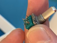
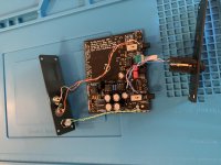
Started my first project, doing an Objective 2 headphone amp (no ODAC). Aside from having some small hang ups and learning pains, it went pretty well and tested perfect. I went to insert it into the case but realized I didn’t cut off the small tab on the potentiometer so couldn’t get it closed. I decided to desolder the pot and cut the tab off. While desoldering, I think I damaged the board.
The pot came out with what looks like one of the copper “cylinders?” on one of the legs. I need to grab more Iso tomorrow to clean it up and get a better look at the board but here are some pictures. Please let me know what you think and how big of an issue it is and how I can repair it.
The pot came out with what looks like one of the copper “cylinders?” on one of the legs. I need to grab more Iso tomorrow to clean it up and get a better look at the board but here are some pictures. Please let me know what you think and how big of an issue it is and how I can repair it.
Attachments
You may be able to join the leg that goes in the damaged hole to the corresponding track on the other side of the board by carefully scraping the lacquer off the track near to the hole and then solder a link between the leg and the track. A thin piece of wire like those on 1/4w resistors would do.
If any of the other holes looks suspect you could do the same. Take a pic of the other side of the board so that we can see it. Rob.
If any of the other holes looks suspect you could do the same. Take a pic of the other side of the board so that we can see it. Rob.
Thanks for the reply. The other holes seem ok and check good for continuity, except the one. They do need to be cleaned up though. The pot also seems to test ok, though I’m not sure I’m testing it right.
Photo of backside of board attached.
Photo of backside of board attached.
Attachments
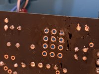
It must be the pics, but I cannot see the tracks either on the top or the underside of the board. I assume that you can see the track from the broken solder pad to the next solder point. As I said earlier when you locate the track very carefully scratch away some lacquer until you see the copper track underneath. You only need to expose a very small area (the size of a pin head will do). It is like undertaking micro-surgery really. These boards are not built to be interfered with and the tracks can lift or split if you go too tough on the scraping.
When you have exposed the track, check for continuity with the next point along the track, then add a small blob of solder to the exposed track. Refit the pot and solder a thin piece of wire to the offending leg of the pot and then solder the other end to the blob on the track. If when testing, the pot is not working correctly check continuity between all the pot pins and the next point along the tracks. It maybe you will need to do more surgery. If you have another board of this type you could practice before going ahead. Rob.
When you have exposed the track, check for continuity with the next point along the track, then add a small blob of solder to the exposed track. Refit the pot and solder a thin piece of wire to the offending leg of the pot and then solder the other end to the blob on the track. If when testing, the pot is not working correctly check continuity between all the pot pins and the next point along the tracks. It maybe you will need to do more surgery. If you have another board of this type you could practice before going ahead. Rob.
Desoldering such potis is always at risk of damaging via platings. To do so select your biggest solder tip, flood all pads with loads of solder, heat it all up and then easy remove the poti. To remove the tab there is no need to remove the poti from the pcb.
It must be the pics, but I cannot see the tracks either on the top or the underside of the board. I assume that you can see the track from the broken solder pad to the next solder point. As I said earlier when you locate the track very carefully scratch away some lacquer until you see the copper track underneath. You only need to expose a very small area (the size of a pin head will do). It is like undertaking micro-surgery really. These boards are not built to be interfered with and the tracks can lift or split if you go too tough on the scraping.
When you have exposed the track, check for continuity with the next point along the track, then add a small blob of solder to the exposed track. Refit the pot and solder a thin piece of wire to the offending leg of the pot and then solder the other end to the blob on the track. If when testing, the pot is not working correctly check continuity between all the pot pins and the next point along the tracks. It maybe you will need to do more surgery. If you have another board of this type you could practice before going ahead. Rob.
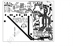
Thanks for the info Rob. The traces are incredibly hard, if not impossible in some spots, to see on this pcb. Looking now though at some of the datasheets (attached below), I see the pin affected connects through the bottom layer to an empty pin 2 rows back. Perhaps the best route may be to solder a wire from the pin on the underside into the other pin slot, if that makes sense.
Desoldering such potis is always at risk of damaging via platings. To do so select your biggest solder tip, flood all pads with loads of solder, heat it all up and then easy remove the poti. To remove the tab there is no need to remove the poti from the pcb.
Thanks for the reply. I started off trying to free the pins individually with a solder sucker and wick but realized that was not really working then I switched to the method you describe here, which worked for me. Unfortunately I think the damage was done on the first attempts. I also had tried to remove the tab with the pot still on but it was not possible for me with my tools without potentially causing damage to the board (ironic...) so I decided desoldering was my best bet.
Attachments
Last edited:
I think you should find that the pot pin with the damaged track attached and the one directly behind it are the earth pins. In the past I have simply joined the two pins together as they are both going to the same ground plane. If there is any track left in the offending hole you can check for continuity with any part of the grd plane. If there isn't then I would join the 2 pins together.

Based on that diagram, this pin, with the damaged hole, is the R+ (to input source) and NOT the ground pin.
This diagram makes sense to me as I had checked the continuity of the ground pin holes and they were good. The only pin not showing any continuity is Pin 3 on the diagram. Perhaps you were viewing the picture at the wrong angle.
This diagram makes sense to me as I had checked the continuity of the ground pin holes and they were good. The only pin not showing any continuity is Pin 3 on the diagram. Perhaps you were viewing the picture at the wrong angle.
Use an OHM Meter
Take an OHM METER switch it to SOUND MODE then as there are 4 Pins on the volume, I think there is might a LOUDNESS SWITCH involved.
Volume controls function that way.
With the ROTATING KNOB facing you and PINS DOWNWARD is
Most left Pin = GND
@Second Pin from left = Output
Third Pin from left = INPUT
and most right pin is Loudness
Try to find the input SOURCE so clip that MEASURE TIP to THIRD from left and then to ground. If you find a resistance, as the Volume Control has been removed, there should be none check the Value of nearby resistors. usually either 47Kohm or 100Kohm and then measure between the two points, from third left to that resistor..
Soon you will figure out which pin is connected to what Part on that board.
And then use a thin wire to make a direct connection
Problem solved.
The same is also true for the output pin of the volume control
Otherwise check if you can find a CIRCUIT Diagram read it and use that thin wire to connect;
Started my first project, doing an Objective 2 headphone amp (no ODAC). Aside from having some small hang ups and learning pains, it went pretty well and tested perfect. I went to insert it into the case but realized I didn’t cut off the small tab on the potentiometer so couldn’t get it closed. I decided to desolder the pot and cut the tab off. While desoldering, I think I damaged the board.
The pot came out with what looks like one of the copper “cylinders?” on one of the legs. I need to grab more Iso tomorrow to clean it up and get a better look at the board but here are some pictures. Please let me know what you think and how big of an issue it is and how I can repair it.
Take an OHM METER switch it to SOUND MODE then as there are 4 Pins on the volume, I think there is might a LOUDNESS SWITCH involved.
Volume controls function that way.
With the ROTATING KNOB facing you and PINS DOWNWARD is
Most left Pin = GND
@Second Pin from left = Output
Third Pin from left = INPUT
and most right pin is Loudness
Try to find the input SOURCE so clip that MEASURE TIP to THIRD from left and then to ground. If you find a resistance, as the Volume Control has been removed, there should be none check the Value of nearby resistors. usually either 47Kohm or 100Kohm and then measure between the two points, from third left to that resistor..
Soon you will figure out which pin is connected to what Part on that board.
And then use a thin wire to make a direct connection
Problem solved.
The same is also true for the output pin of the volume control
Otherwise check if you can find a CIRCUIT Diagram read it and use that thin wire to connect;
Based on that diagram, this pin, with the damaged hole, is the R+ (to input source) and NOT the ground pin.
This diagram makes sense to me as I had checked the continuity of the ground pin holes and they were good. The only pin not showing any continuity is Pin 3 on the diagram. Perhaps you were viewing the picture at the wrong angle.
Woops. You are of course right. Apologies I should have looked again at the picture of you holding the pot!
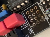
There are 12 holes to connect a potentiometer with 6 pins, six of which are marked "15 mm" and six marked "20 mm". Hopefully the six holes marked "20 mm" are connected to the same nets as those marked "15 mm", but are meant for longer potentiometers. Maybe you can then connect the pin that goes into the damaged hole to the corresponding hole for 20 mm potentiometers using a short wire. In that case you don't even have to scratch off any solder mask.
There are 12 holes to connect a potentiometer with 6 pins, six of which are marked "15 mm" and six marked "20 mm". Hopefully the six holes marked "20 mm" are connected to the same nets as those marked "15 mm", but are meant for longer potentiometers. Maybe you can then connect the pin that goes into the damaged hole to the corresponding hole for 20 mm potentiometers using a short wire. In that case you don't even have to scratch off any solder mask.
This is what I was starting to think. I confirmed that it shares a trace with the hole 2 rows behind it. My only concern now, as I lack the knowledge: is this possibly problematic if it manages to make an intermittent connection in the original hole? So it would have a connection at two points potentially. Is that even possible or a potential issue? Hope that makes sense
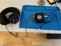
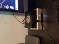
I ended up connecting the pin with a wire to the hole 2 pins behind it and it worked great. Project finished! A bit of a Frankenstein... not the best solder job, tight fit in the case, small ugly wire job connecting poti, and a few minor pcb scratches. BUT it all tests good, works as expected, and sounds great. I'll post a few pics of it later.
Thanks for the help everyone!!
Thanks for the help everyone!!
Some final build photos as promised. Note the ugly-looking wire on the poti that I put a small coating of liquid elec tape on in case of rubbing. All tests and works good tho! And don't worry, I cleaned it up some lol
Attachments
-
 FABC2025-334F-4554-A8E4-4F254C8A02C1.jpg592.9 KB · Views: 63
 -
 9DB1224C-5BA0-483C-B3B1-830DAD08B254.jpg819.6 KB · Views: 72
 -
 70433063-0201-463B-BE76-09E934D86CB0.jpg750.7 KB · Views: 89
 -
 65D304A7-7748-48E0-A9EF-909609FAFDD8.jpg764.8 KB · Views: 80
 -
 D745A681-81DE-47F3-A4CF-E1F498F19EFD.jpg875.6 KB · Views: 73
Last edited:
- Home
- Amplifiers
- Chip Amps
- Damaged PCB? Help!