I have two serious concerns regarding the circuit you are planning to build. The first is that the transformer will not present a 46 ohm load to the DAC, it will present a 300 ohm load. Which means that there would be about a 1.1V pk-pk swing at each PCM1794A output pin. While I don't know the low distortion compliance limit of the PCM1794A outputs, I feel fairly certain that you would exceed or be flirting with it.
Could you show your calculation arriving at the 300 ohm load?
As far as I can see the reflected 46 ohm load is in series with the DCR of the primary, which is 92 ohm when I check the datasheet of the transformer.
That would give some 140 ohm source impedance.
The second concern is that without an i/v resistor in parallel with the DAC output to establish a reasonable source impedance for the primary, the source impedance will be very high, on the order of a couple megohms for the PCM1794A according to reports I've read. This will cause the transformer to generate very significant distortion.
Curious for that "reports you have read".
The former PCM63 has 680 ohm output impedance; the current PCM1704 has 1k output impedance. I don't believe that the PCM1794 with it's differential current outputs will have an output impedance in the order of mega-ohms; will be more likely to be some 1k.
I suppose, that the only way you are going to learn is to find out the hard way.
IMHO we are here to encourage, not to discourage....
Dirk, my advice, as mentioned before, to put the I/V resistor right at the output of the DAC (best in my experience).
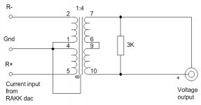
According to the Sowter math, I get the following:
DAC output current: 7.8mA p-p
Current in transformer secondary, Is = 7.8/4 = 1.95mA p-p, 0.689mA RMS
if Rg (I/V resistor) = 750ohms, Rg=Vg/Is, Vg = 0.517volts
op amp gain stage is about 4: output = 0.517*4 = about 2 volts.
reflected impedance on DAC for 750 ohms:
750/16 = 47 ohms
DAC output current: 7.8mA p-p
Current in transformer secondary, Is = 7.8/4 = 1.95mA p-p, 0.689mA RMS
if Rg (I/V resistor) = 750ohms, Rg=Vg/Is, Vg = 0.517volts
op amp gain stage is about 4: output = 0.517*4 = about 2 volts.
reflected impedance on DAC for 750 ohms:
750/16 = 47 ohms
Dirk, my advice, as mentioned before, to put the I/V resistor right at the output of the DAC (best in my experience).
Thanks. I'll experiment with that eventually.
So, are you saying that the math as presented by Sowter is incorrect? How did you arrive at your number? I showed in a previous post exactly how I did it, and yet you just blurt out some number without any math to back it up.
Second, do you think for a minute that Sowter would risk their reputation by publishing something that was completely wrong or otherwise unworkable?
Firstly, I showed you an example of the math for calculating the transformer impedance in a prior post within this very thread. I'll briefly repeat it here, except now, using your latest circuit with the Jensen JT-10KB-D transformer as a 1:4 step-up, just as I had suggested.
1) The net secondary load would be 47 ohms + 750 ohms + the secondary winding resistance (wired 1:4 step-up) of 2,500 ohms = 3,297 ohms.
2) The reflected impedance then is 3,297 ohms / square of the turns ratio (16) = 206 ohms.
3) Net load presented to the DAC is 206 ohms + the primary winding resistance of 92 ohms = 298 ohms. So, I blurted out nothing.
Secondly, my assessment of your circuit has nothing to do with Sowter's circuit. It has to do with your using a different transformer than Sowter, along with a DAC which is reported to have a very high output impedance and which you don't know the output voltage compliance for.
In short, you simply have to account for multiple and inter-related factors in electronic engineering, just as you would in mechanical engineering. So far, you have showed surprisingly little patience (and humility) with learning what you need to know about electronics.
Last edited:
Could you show your calculation arriving at the 300 ohm load?
As far as I can see the reflected 46 ohm load is in series with the DCR of the primary, which is 92 ohm when I check the datasheet of the transformer.
That would give some 140 ohm source impedance.
Please see my latest reply to dirkwright for my 300 ohm calculation.
Curious for that "reports you have read".
The former PCM63 has 680 ohm output impedance; the current PCM1704 has 1k output impedance. I don't believe that the PCM1794 with it's differential current outputs will have an output impedance in the order of mega-ohms; will be more likely to be some 1k.
I seemed to recall reading that on one of the DIY blogs somewhere, but I very well may not recall this correctly. In any case, and as I'm sure you know as well as anyone, low impedance transformer primaries should be driven from a lower impedance source, assuming that minimizing distortion is an design criteria.
Whatever is the actual impedance of the PCM1794A current output, it most certainly isn't close to 300 ohms, let alone even less than that.
Last edited:
IMHO we are here to encourage, not to discourage....
Pieter, I very much agree with that sentiment. If you take a look at my first three comments within this thread in support of dirkwright's project, I think you'll see that. What I won't do, however, is encourage pointlessly stubborn behavior.
Last edited:
Pieter, I very much agree with that sentiment. If you take a look at my first three comments within this thread in support of dirkwright's project, I think you'll see that. What I won't do, however, is encourage pointlessly stubborn behavior.
So, I'm just supposed to roll over and do as you say like I'm a good dog or something?

Nevertheless I encourage Dirk to go on the way he does.
Sowter specifies their 1:12.8 DAC step up transformer to function just like Dirk describes (Sowter is neither impatient nor stubborn).
Then we have K&K Audio which implemented a 1:4 Lundahl step up transformer (driven by the same PCM1794 by the way...) with exactly the same equations (PCM1794 has 2.75 mARMS - secondary of the 1:4 was loaded by 3k giving the standard 2 VRMS).
Then we have me who had a commercial Dac some 12 years ago; PCM63 with 100 ohm I/V converter at the dac chip output followed by a 1:5 step up transformer providing exactly the calculated RMS voltage at the secondary (1.4x100x5 = 700 mVRMS).
Your calculation reminds me of the way I calculate secondary impedance of power supply transformers, however your calculation of "net secondary load" is not correct; should be (primary DCR x winding ratio ²) + secondary DCR.
Last edited by a moderator:
Nevertheless I encourage Dirk to go on the way he does.
Sowter specifies their 1:12.8 DAC step up transformer to function just like Dirk describes (Sowter is neither impatient nor stubborn).
I said to dirk, my assessment of his circuit has nothing to do with Sowter's circuit, or Sowter's attitude disposition. 😉
Ah, I just see Dirk's post confirming my example of the K&K kit.
Seriously, guys, this is rather simple. My point is simply that you cannot arbitrarily take someone elses schematic, alter it without understanding the engineering relationships, and safely go off on your merry way. Well, one can do that, but avoidable heartbreak may, and eventually will, follow. I've absolutely NO interest in forcing (contrary to as dirk believes) anyone to follow my suggestions. Dirk is entitled to his own listening preferences, but he is not entitled to his own circuit physics. We are all here to both learn and teach, but mostly to help each other. That is what I was attempting to do for dirk. Something which I will cease, after this final reply.
That K&k output stage is actually designed by a company called Raleigh Audio. The transformer used therein is a Lundahl LL1674. To get a 1:4 ratio with the LL1674 both primaries and both secondaries would be paralleled. So, for what will be the last attempt by me to get this point through, let's find the impedance seen by the DAC in this LL1674 based output.
1) Net secondary load is 3k + the paralleled secondary winding resistance of about 302 ohms.
2) Reflected impedance will be 3,302 ohms / square of turns ratio (16) = 206 ohms.
3) Net primary load (as seen by the DAC) will be 206 ohms + the paralleled primary winding resistance of about 16 ohms = 222 ohms.
This impedance presented by dirk's JT-10KB-D based circuit is almost 50% higher than for the K&K LL1684 based circuit. Which means the output voltage at the PCM1794A would by higher by that same percentage. Is that too much voltage swing? Will it cause the PCM1794 to distort unacceptably? Will the DAC's less than ideal output impedance needlessly produce distortion? The answer may be yes, the answer may be no, but why even try? Why not simply place a resistor at the DAC output to both limit the voltage swing AND lower the source impedance.
Last edited:
Just so you know, the Twisted Pear COD offers an optional passive I/V converter on board which uses 392ohm resistors.
Actually, the schematic for the Twisted Pear COD I/V resistor network is attached, and uses 470ohm resistors. This is not a critique or comment on the COD DAC at all, just an observation that Twisted Pear appears to be comfortable with a resistive load on the DAC of 392-470 ohms per leg of the balanced output so I don't see where a load of 300 ohms presented by my circuit should be a problem.
Attachments
Seriously, guys, this is rather simple. My point is simply that you cannot arbitrarily take someone elses schematic, alter it without understanding the engineering relationships, and safely go off on your merry way. Well, one can do that, but avoidable heartbreak may, and eventually will, follow.
That is your personal truth but not necessarily a universal one.
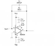
Here's part of the I/V converter as suggested by TI in their data sheet for the PCM1794A. The equation for determining the maximum voltage at the Iout pin is given by:
Vi=7.8mAp-p*R1
As can be seen in the figure, R1=750ohms, giving a full 2volts RMS at the output pin. The unshown stage following this one has unity gain. So, I think that there is plenty of headroom in the circuit I designed. The data sheet goes on and shows another I/V converter with an even higher R1 leading to a full 4.5volts RMS output.
One concern I have right now is whether or not the current output pins need to be DC connected to ground, either through a transformer or a resistor. The Sowter web page does not show a ground connection and I'm not sure about other designs out there. The data sheets and other technical documents I have read seem to indicate that a ground connection is required so I may have to add the resistors on the primary side of the transformer after all, but the full figure for the I/V and balanced to unbalanced conversion do not show a ground connection for the minus Iout pin. So, I'm confused about that right now.
Attachments
Last edited:
- Status
- Not open for further replies.
- Home
- Source & Line
- Digital Line Level
- DAC project