I'm thinking of designing my first DAC. One question I grapple with:
Do I consider the analog section as anlog in the broadest sense? Does common wisdom regarding analog circuits, like i.e. buffers, preamps etc. apply here too?
For the digital section I'm profoundly convinced that the use of SMD components is the way to go - Keep it all as tight as possible to achieve small loop areas in decoupling, use groundplanes etc. etc. ... But on the analog side - Is there a higher degree of freedom; is the use of through-hole parts non-critical, do I use star-grounds? For the I/V or buffer stage it's quite obvious, my question only concerns the analog voltage supply pins, analog reference decoupling, quiescent voltage filtering etc..
I've been looking at many implementations of DAC circuitry, but I can't recognize any rule. 😕
Last edited:
look up "grounding high resolution convertor" on Google, you will get plenty of information regarding the grounding of mixed signal systems.
if you are using SMD for the digital (best choice) you can use SMD for the analogue side, though there are numerous arguments over PTH vs SMD. I do layout for some quite interesting DACs and SMD is used in the output. Get the right components and SMD output with op-amps is possible.
Here are a few good links, there are many more and each device will have some recommendations in the data sheets.
Grounding of Mixes Signal Systems
http://www.analog.com/static/imported-files/tutorials/MT-031.pdf
http://www.ti.com/general/docs/lit/getliterature.tsp?genericPartNumber=ads1282-ht&fileType=pdf
http://www.ti.com/lit/an/sbaa052/sbaa052.pdf

If you were to follow all these SMART manuals how to rout PERFECT PCB, you would never finish you project. All these manuals are good for very quite simple circuit. Say, you have 4 chips, everyone of them has analog, digital part, auxiliary pins and so on. Plus you have 4 power supply, than few OP Amps, than Amplifier for heads.
Now, try to reed it and make perfect PCB. I bet you will spend few weeks and end up in deepest depression cause all these manuals say are very contradictory.
=)
Now, try to reed it and make perfect PCB. I bet you will spend few weeks and end up in deepest depression cause all these manuals say are very contradictory.
=)
Sorry but I have to disagree, people especially like Henry Ott write these articles and books to guide you, that is the only way to learn the complexities of todays PCBs.
And no these manuals are good for more than 4 chips, I use them and boards I lay out have more than 4 chips, a lot more and are of an order more complex than an Audio DAC design.
Here's another very good link that explains the basics of how signals travel on PCBs:
http://www.x2y.com/filters/TechDay0...log_Designs_Demand_GoodPCBLayouts _JohnWu.pdf
For digital a solid contiguous ground plane is best, depending on the complexity of the design you can use 2 layers for simple designs and still get a solid ground plane (ES9023) for more complex designs a 4 layer board is preferable. Analogue benefits from a ground plane, star grounds are not the best solution and never have been, but more-so now with so much RF noise around.
The info I have presented is only a small fraction of the info out there, though if you have to follow any, H.Ott is the man.
I don't understand why such a negative attitude towards the information given Devilsdance7775, how would you propose people start learning about mixed signal design?
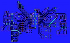
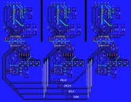
My take on Marce's hints and the schematic it is based on. My version is for two layers, it has continuous copper pour on both sides and is meant for homemade PCB. I'll use I2S input only, output stage will be on a separate board. I know there should be significantly more via stitches, I show only the most important ones for better perceptibility.
The layout is not really ready yet, I2S input will be with U.FL coaxial cabling and so the input pads have to be altered accordingly.
This is my first attempt, so please be indulgent.
The layout is not really ready yet, I2S input will be with U.FL coaxial cabling and so the input pads have to be altered accordingly.
This is my first attempt, so please be indulgent.
Attachments
Last edited:
Remove thermal relief from your vias.
Boards will be homemade, so no plated-through vias. Might be hard to solder without thermal reliefs ...
> Do I consider the analog section as anlog in the broadest sense?
Everything is analog (including digital).
Digital is just a particular kind of analog with very high noise tolerance, high di/dt, and potential for generating high levels of noise on your board.
If your board contains only slow digital stuff (high noise immunity, not too much noise generation) you can think "digital", it will work (more or less) even with 1 volt of crap on all signals (disregarding EMC regulations). If your board has high-speed digital (much higher noise generation) and analog circuits handling microvolts (like a 24 bit DAC) you can't really afford to think "digital"...
For example, since your DAC chip isn't an abstract, perfect theoretical entity, but a real piece of silicon, there will be glitches, clock feedthrough and other crap on the output.
Now :

Any RF crap on the DAC output is injected directly into the opamp input.
What is above the opamp's GBW will make it choke.
However, if you use a fast opamp, new audio ones have 50 MHz GBW, you may think it will be OK, anything below 50 MHz will be processed by the opamp, the output will stay controlled and continue to present a virtual ground to the DAC output thru the feedback capacitor.
But for this to happen, among other things :
1) The opamp's power supply should have a proper low impedance at those frequencies... opamp GBW from datasheet depends on the supply being stiff, not an inductor. With high power supply impedance, bad stuff happens.
IMHO this pretty much makes proper decoupling at this opamp's supply mandatory, which means SMD ceramics... not the famous big red plastic caps...
2) The feedback cap should also not be an inductor... including its connections to the opamp. I'd use C0G ceramic.
Anyway, you're not using an IV, so this was just for the example.
> Boards will be homemade, so no plated-through vias.
COME ON !!! Please.
ITEAD Studio 2Layer Green PCB 10cm x 10cm Max
Problems in your design :
- No output filter
RF crap emitted by the DAC on the output should not be permitted to leave the boadd. A simple RC filter with SMD caps (NP0 or PPS) will do.
- Clock is in the wrong place
But you probably can't do anything about it...
Problems in your layout :
1- No ground plane
2- decoupling is weak (consequence of point 1) using high inductance long skinny traces
3- Connectors
You need to rework your connectors. For example, the output is balanced so it will be twisted pair, where is the shield connected ? I see no ground connection... Also both shields should connect to the same spot or your cables will have common mode....
Same for input connectors, where are the grounds ?
Everything is analog (including digital).
Digital is just a particular kind of analog with very high noise tolerance, high di/dt, and potential for generating high levels of noise on your board.
If your board contains only slow digital stuff (high noise immunity, not too much noise generation) you can think "digital", it will work (more or less) even with 1 volt of crap on all signals (disregarding EMC regulations). If your board has high-speed digital (much higher noise generation) and analog circuits handling microvolts (like a 24 bit DAC) you can't really afford to think "digital"...
For example, since your DAC chip isn't an abstract, perfect theoretical entity, but a real piece of silicon, there will be glitches, clock feedthrough and other crap on the output.
Now :
Any RF crap on the DAC output is injected directly into the opamp input.
What is above the opamp's GBW will make it choke.
However, if you use a fast opamp, new audio ones have 50 MHz GBW, you may think it will be OK, anything below 50 MHz will be processed by the opamp, the output will stay controlled and continue to present a virtual ground to the DAC output thru the feedback capacitor.
But for this to happen, among other things :
1) The opamp's power supply should have a proper low impedance at those frequencies... opamp GBW from datasheet depends on the supply being stiff, not an inductor. With high power supply impedance, bad stuff happens.
IMHO this pretty much makes proper decoupling at this opamp's supply mandatory, which means SMD ceramics... not the famous big red plastic caps...
2) The feedback cap should also not be an inductor... including its connections to the opamp. I'd use C0G ceramic.
Anyway, you're not using an IV, so this was just for the example.
> Boards will be homemade, so no plated-through vias.
COME ON !!! Please.
ITEAD Studio 2Layer Green PCB 10cm x 10cm Max
Problems in your design :
- No output filter
RF crap emitted by the DAC on the output should not be permitted to leave the boadd. A simple RC filter with SMD caps (NP0 or PPS) will do.
- Clock is in the wrong place
But you probably can't do anything about it...
Problems in your layout :
1- No ground plane
2- decoupling is weak (consequence of point 1) using high inductance long skinny traces
3- Connectors
You need to rework your connectors. For example, the output is balanced so it will be twisted pair, where is the shield connected ? I see no ground connection... Also both shields should connect to the same spot or your cables will have common mode....
Same for input connectors, where are the grounds ?
And no also peufeu is in - This might become very educational 🙂
In the end everything is analog, so much I understood.

It's all tad bit better that way?
In the end everything is analog, so much I understood.
No opamps, but transformers. Should have mentioned that. The analog peripherals are very clear to me, but thank you anyway.Any RF crap on the DAC output is injected directly into the opamp input.
I agree ...COME ON !!! Please. ITEAD Studio 2Layer Green PCB 10cm x 10cm Max
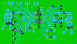
Indeed, I cant. I'll tap into the I2S lines of a Behringer DCX2496.- Clock is in the wrong place. But you probably can't do anything about it...
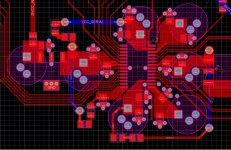
It's down there, the green one is the bottom layer (x-ray view). Only the fewest vias are drawn in yet.Problems in your layout: 1- No ground plane
Connectors will be coaxial U.FL, shields tied to ground on both sides. Have drawn them in now on the top layer (blue):3- Connectors
That's definitely not the final version of the layout ...You need to rework your connectors. For example, the output is balanced so it will be twisted pair, where is the shield connected ? I see no ground connection... Also both shields should connect to the same spot or your cables will have common mode....
It's all tad bit better that way?
Attachments
Last edited:
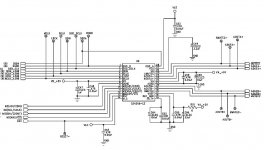
Just looked at the datasheet and found some mistakes in your schematic :
- VREF is a input, should come from AVCC
- The various VCCs for IOs (serial and control) of the chip must be supplied, at the voltage actually used for IO. 3.3V I guess. DVCC can also be 3.3V, should be less noisy than 5V.
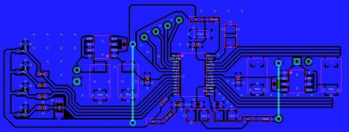
And... I had some free time so here's a quick try at a layout...
See attached files. I can upload Altium files if you want.
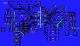
I've used 2 layers.
Top has ground fill everywhere (removed in some pictures for clarity).
Bottom is solid ground plane, no tracks.
This is just a quick layout, I did not spray ground vias everywhere as would be needed.
The blue tracks are not actually tracks... they would be wire jumpers. When assembling just one board, adding a few jumpers isn't a problem, and it is much better than cutting the ground plane.
However routing a wire (or a track) between two decoupling caps makes a CLC which must be broken with a little ferrite bead. It's either a few $0.01 ferrites or a 4 layer board with ground and power planes, so I put the ferrites.
I've used SOT223 LDOs cause I had the pcb footprint at hand.
All big caps are 8mm diameter thru-holes on the other side of the board, so they don't get in the way. Another thing you can do for homemade protos.
All power pins go to a small copper pour (low inductance) with decoupling caps on it.
I included a filter at the output (here a X2Y ceramic C0G cap), or SMD PPS film caps, etc.
Notice MCLK trace isn't hugging the others (crosstalk = jitter).
I've put ribbon cable headers... by default.
> No opamps, but transformers.
OK, good.
Note RF noise goes straight through interwinding capacitance, so a little bit of filtering at the DAC output is still needed. Putting the footprints for a RC filter on the PCB is free...
On your last layout all the DACs use the same data line from the behringer... ?
The cuts in ground plane at the top do no good. It is better to be sure all wires leaving the board will have the same common mode voltage.
Also, those UFL coax... hm... you're source-terminating them at the other side, right ?
- VREF is a input, should come from AVCC
- The various VCCs for IOs (serial and control) of the chip must be supplied, at the voltage actually used for IO. 3.3V I guess. DVCC can also be 3.3V, should be less noisy than 5V.
And... I had some free time so here's a quick try at a layout...
See attached files. I can upload Altium files if you want.
I've used 2 layers.
Top has ground fill everywhere (removed in some pictures for clarity).
Bottom is solid ground plane, no tracks.
This is just a quick layout, I did not spray ground vias everywhere as would be needed.
The blue tracks are not actually tracks... they would be wire jumpers. When assembling just one board, adding a few jumpers isn't a problem, and it is much better than cutting the ground plane.
However routing a wire (or a track) between two decoupling caps makes a CLC which must be broken with a little ferrite bead. It's either a few $0.01 ferrites or a 4 layer board with ground and power planes, so I put the ferrites.
I've used SOT223 LDOs cause I had the pcb footprint at hand.
All big caps are 8mm diameter thru-holes on the other side of the board, so they don't get in the way. Another thing you can do for homemade protos.
All power pins go to a small copper pour (low inductance) with decoupling caps on it.
I included a filter at the output (here a X2Y ceramic C0G cap), or SMD PPS film caps, etc.
Notice MCLK trace isn't hugging the others (crosstalk = jitter).
I've put ribbon cable headers... by default.
> No opamps, but transformers.
OK, good.
Note RF noise goes straight through interwinding capacitance, so a little bit of filtering at the DAC output is still needed. Putting the footprints for a RC filter on the PCB is free...
On your last layout all the DACs use the same data line from the behringer... ?
The cuts in ground plane at the top do no good. It is better to be sure all wires leaving the board will have the same common mode voltage.
Also, those UFL coax... hm... you're source-terminating them at the other side, right ?
Attachments

You're the man, peufeu!  Many, many thanks!
I'll make another layout attempt tonight or tomorrow morning.
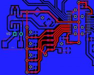
Many, many thanks!It's not easy to recognize, but it does so, AVCC path accentuated in red... (1st pic)- VREF is a input, should come from AVCC
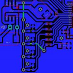
They are also supplied (2nd pic). The M0-M3 lines are routed either to DVCC or ground, selectable by kinda "solder blob jumper" (3rd pic)- The various VCCs for IOs (serial and control) of the chip must be supplied, ... ...
Many thanks again! I'll use it as a guideline and implement it's routing into my next draft.And... I had some free time so here's a quick try at a layout...
Beyond question.Putting the footprints for a RC filter on the PCB is free...
Oops! 😱In your last layout all the DACs use the same data line from the behringer... ?
Understood!The cuts in ground plane at the top do no good. It is better to be sure all wires leaving the board will have the same common mode voltage.
Of course!Also, those UFL coax... hm... you're source-terminating them at the other side, right ?
I'll make another layout attempt tonight or tomorrow morning.
Attachments
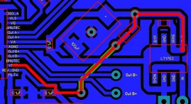
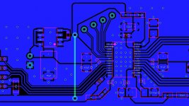
Looking better, but the decoupling cap is to far from the pins.
Make your signal tracks a bit thinner on the digital signals, also up the spacing, you run the risk of cross talk and have no room to move them out of the way to get the cap nearer.
A good rule of thumb is w/w for signals, where the track and gap is the same, and for clock signals w/3w where possible try and leave 3 times the track width between clock signals and any other trace, pad or via. This then allows a guard trace around the clock if required.
Marce, what do you think about the layout I posted earlier ? (I'm taking the occasion to learn from the pros 😉
To get the signal traces out of the way of the power pours as quick as possible and make room for decoupling caps, you can use the thinnest track/space available close to the chip. Further away when it gets less cramped, more space means less crosstalk. For 20$ you get 8/8 mil track/space or even less these days...
Also, now, we get 10x10cm 4 layer boards for less than $80. You got to ask yourself, is the extra time worth it to get a good 2 layer layout ? If you use 4 layers you can save a weekend of slaving over the layout... maybe worth the price difference... IMO 4 layers makes even more sense for small DIY projects, you're not gonna make a million boards and try to shave pennies, it's just an extra cost (about $50 versus 2 layer) versus much faster and easier layout...
- Status
- Not open for further replies.
- Home
- Source & Line
- Digital Line Level
- DAC parts selection - Do I consider analog as anlaog in the broadest sense?