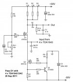
I plan to build a DAC using 4 TDA1543 in parallel, coupled with a Pass Lab D1 I/V stage. The concept schematics is attached and would like to invite advices and comments.
These are my considerations in making the schematics:
The full scale current (sink) output of TDA1543 is 2.3mA, so with 4 in parallel, this will be close to 10mA. With a 1.5k Ohm drain resistor in D1, this will give 15V voltage swing, which is too much. Also, the D1 bias setting would not allow such a voltage swing. So a scaling process is required. Instead of using a scale factor of 4x (which looks obvious by with 4 DACs in parallel), I use 3x to get a bit more gain
The drain resistor is hence reduced from 1.5k to 500 Ohm. I use 3 1.5K resistor in parallel to get the 500 Ohm effective resistance. I believe this will statistically reduce the deviation and give a more accurate 500 Ohm for the I/V conversion (matching between L and R will be better)
The bias current of 10mA in D1 will give a voltage drop of 5V across the 500 Ohm, this is too low. I increase the bias current to 30mA. This can maintain the output DC level at 15V, also should improve the linearity by biasing the IRF610 harder.
With a 30mA bias, the source resistor of 3.3k in D1 should be reduced to 1.1k. This appears to be quite low and I believe this will reduce the robustness of the constant current flow from the source pin to -30V. I change this to a CCS.
The output LPF is kept after the 10uF blocking capacitor. The values are taken from the Zen I/V design
In the original D1, there is a input capacitor of 0.01u at the input. I am not sure if this is required (C4 in my schematics)
The TDA1543 would like to see its output biased to a voltage at Vref (2.2V). By trimming the pot at the gate, I will set the source potential at 2.2V (or measured 0V between this pin and the Vref pins of TDA1543)
The input to the DACs will be from 2 I2S sources: a USB input via PCM2707, and a SPDIF input via CS8414.
Attachments
I would like to know also, unfortunately the project is still at the drawing board stage. Will take a while to get the parts and have it built up.
Yes, this method is very much documented in the web and in fact I do own 1 TDA1543 based DAC now which use a single resistor as I/V. I am however not impressed by the sound and hence would like to see if changing the I/V setup can bring something new. Of course there can be other reasons behind the dissatisfaction, but this I/V stage change can serve as step 1 of the exploration.
Some upates.
I finally build the DAC and make some audition today.
Compared to the single resistor setup, I found this D1 I/V stage to be less "grainly". Depth and transparency are good, and I am very happy with the result.
With the component I got at hand, the bias current of the IRF610 is almost 40mA now. They are really working hard.
Yes, this method is very much documented in the web and in fact I do own 1 TDA1543 based DAC now which use a single resistor as I/V. I am however not impressed by the sound and hence would like to see if changing the I/V setup can bring something new. Of course there can be other reasons behind the dissatisfaction, but this I/V stage change can serve as step 1 of the exploration.
Go for TDA 1541A and you will be happy. You ill never be happy with TDA1543 when it comes to serious music listeing expirence.
- Status
- Not open for further replies.
- Home
- Amplifiers
- Pass Labs
- D1 I/V with 4x TDA1543