Dear Dave,
very interesting project!
BTW: I can confirm that your IXYS simulation models for IXTH80N20L and IXTH48P20P work pretty well. The breadboard test sample works very stable.
The cooling of those devices need to be very good if you want to drive them in the near of their maximum pd - I have killed the P-channel device during heavy bias test because of bad cooling 😉
BR, Toni
P.S.: here the link to the schematic of the working test sample
That's what I started with. The 'final' values were arrived at after trying 2R loads and overload.If you can land the phase peak directly on top of the ULGF, that would leave you closer to 60.
Have you tried added stray capacitance on the power supply to see what it does to stability?
It's all very early days for me.
With the conventional Blameless & my pure Cherry versions, I was confident of my results cos LTspice was replicating practically everything I encountered in 'real life'.
With V&K, I have no 'real life' to compare with and am somewhat surprised at how suspicious I am of its predictions.
They also form nice NDFLs
It's hardly a full blown NDFL amp. I look at Cherry's NDFLs as just a 'convenient' way to approach Bode's max feedback.I am not convinced by the whole NDFL concept, despite my respect for Dr Cherry.
Having only 2 'devices' in series means each 'block' is unconditionally stable if you ignore load ... and the differentiating feedback deals with that.
In fact my 'pure Cherry' has 4 devices; the enhanced VAS and the EF2 while Cherry's examples (eg the ETI amp) has 3 devices. My V&K has only 2 devices so I should dub it PUREST CHERRY 😀
but bUT BUT ... isn't my Tian probe in the right place? It cuts all 3 feedback loops.The position you have looks essentially correct but Tian probe is theoretically not quite correct.
Usually this makes no practical difference but I am not sure about this case because the feedback loops are interconnected.
Why do my friends always do the most complicated compensation😉
There's loadsa new stuff to learn with this.
One important HF distortion mechanism which it avoids is yucky Ccb modulation of the VAS. Its collector doesn't move much. I think that's why the V&K version outperforms the 'conventional' topology it is based on by quite a bit.
The amp looks very 'textbook'. IP transconductance, Current Amp (the old VAS), '2 more current amps arranged as an integrator'
But do you need both C1&7? Why is the remaining THD mostly 2nd at LF? What are the worst case loads for stability? Do we need the 4r7 base resistors on the output devices which are no longer EFs?
____________________
Now that's timely. I was going to ask if there were some Spice models for power FETS that didn't come from Ye Olde Unobtainium Shoppe.I did LTSpice VDMOS models with the latest sub-threshold parameters.
Toni did his usual excellent build, it's in his thread, summary is that the models worked well and so do the transistors.
They look ideal for a CE/CS amp, the ~4 V threshold ceases to be a problem and becomes actually useful.
I can send you the preliminary models if you want, not ready to release them publicly until I have checked them some more.
I've got LTspice 4.22w 18feb2015. Do I need to upgrade to use these models?
It's hardly a full blown NDFL amp. I look at Cherry's NDFLs as just a 'convenient' way to approach Bode's max feedback.
It is not hard to show that NDFL is theoretically sub-optimal.
But maybe it is a convenient way to approach max feedback.
but bUT BUT ... It cuts all 3 feedback loops.
Yes, as I wrote, essentially correct, that's the best place for it, for sure.
The problem is that it doesn't quite cut all 3 feedback loops.
There is also transmission via C1+C7 and C4, back to the base of Q14.
And also the other way, forward to the bases of Q1 and Q2.
Not to mention from C1+C7 via R6 + C3 to the base of Q4.
And more paths can be found.
Tian does not consider these absolutely accurately.
This shows up most obviously as "weird" phase behavior, like in Damir's circuit that we all discussed a while back.
Normally the difference is trivial but I would like to be able to do this strictly.
In the past I have probed multiple points and eyeballed each result.
Really I should use maths to combine the results
I have finally started to understand this last hurdle.
Theory says there aren't any more layers of complexity to unpeel, at least in linear model.
...if there were some Spice models for power FETS that didn't come from Ye Olde Unobtainium Shoppe.
You mean the Spice models are Unobtainium or the FETs?
Toni already has the FETs, from Mouser, about $10 each, not bad for 500 W devices.
The models are from me, free😉
I should have some transistors on the way too.
LTspice 4.22w 18feb2015.
I am almost sure that's sufficiently up to date.
LT's code has been ready a while, the problem has been almost no models used the new parameters.
Best wishes
David
Last edited:
shows plenty of excess loop gain...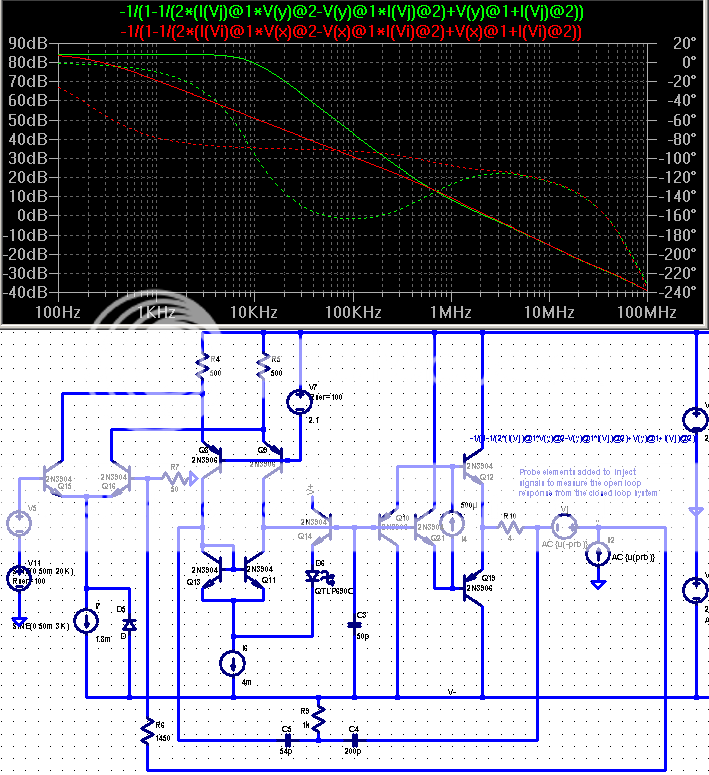
Hi John
The recent start of a similar thread prompted me to look back over this one, and I noticed an issue that I missed the first time.
Your Tian probe in the above schematic doesn't capture the full feedback because it misses the parallel path that splits off earlier.
I think this is prone to misinterpretation, did you consider the full path?
Best wishes
David
"inside everything" only shows that the OL gain is "the same" up to loading effects
I think the point was the difference in gain availble "outside" the compensation loop - as would be available to correct a unity buffer
http://www.diyaudio.com/forums/solid-state/123613-class-biasing-ad797-6.html#post1525757
but at this later date I could possibly be talked around to another view
I think the point was the difference in gain availble "outside" the compensation loop - as would be available to correct a unity buffer
http://www.diyaudio.com/forums/solid-state/123613-class-biasing-ad797-6.html#post1525757
but at this later date I could possibly be talked around to another view
...I think the point was the difference...
Thanks, the link makes clear that you did indeed consider it, that was my main question.
Now I will study the post more carefully.
Best wishes
David
Guru Zan,
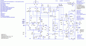
I've done a bit more work on my V&K variant. I spent a lot of time trying to find the major sources of THD .. particularly the dominant 2nd harmonic.
Cascoding everything in sight made little or no difference.
Cordell current loads for the input LTP made the only big difference .. dropping THD for most of the audio band to 1ppm ... mainly due to increased loop gain.
THD20k is 5ppm ... the 20kHz sinewave on the last pic is the input reduced to 0.01%. Actual output is 20V 8R ie 50W
I think this uses every dB of LG possible from 3 stages + i/p LTP. Adjust ULGF for whatever stability criteria you favour .. which will mostly affect the top 8ve.
The remaining THD is all due to hfe mismatch of the output stage. You can't do much about it without introducing more gain stages & more wonky stability. If you use extra feedback on one half to reduce its hfe advantage, you are really just getting rid of some LG which might help stuff universally.. and convert 2nd harm to nasty 3rd
I'll show the effects of Voltage & Current Drive on this output stage later this month.
Much of the work has been twiddling R1,2, 14,19, 7,17 & R21 to see if the push pull VAS could be improved. Also stuff to improve overload.
Dunno if this is the optimum topology for V&K. It's likely an even simpler circuit might give even better results.
Attachments
Last edited:
Hi!
Do the tubes suffer from excessive crossconduction distortion in AB class transformer output stages?
Do the tubes suffer from excessive crossconduction distortion in AB class transformer output stages?
...I've done a bit more work on my V&K variant.
I'd say you have done more than a bit more work, looks serious to me.
What does the loop gain plot look like?
And what does it look like when you load the power supply with some stray capacitance?
If stray power supply capacitance is actually a problem then is there any reason why the OPS circuit could not be inverted into a Common Emitter with the emitters connected to the power supply rails, a la Cherry's article?
Thanks for the enthusiasm, my AD797 idea is stuck so I'm a bit disappointed at the moment. The Bryston looks OK however and I will post it soonish
Best wishes
David
C1/C7 complicate the loop gain picture a little, maybe an issue to watch.
Not sure whether R16/R30/C6 need some loop gain check.
Would D2 be better replaced by a diode connected transistor? the only real cost would be to the claim of how few transistors you use.
Last edited:
I think that this kind of load was invented by Widlar and is based on a common mode loop. This scheme can be found in one of the Groner's circuits.Cordell current loads for the input LTP made the only big difference .. dropping THD for most of the audio band to 1ppm ... mainly due to increased loop gain.
When adding two emitter followers ahead the differential VAS (Q14-Q16 in your schematics), simulations I made a few weeks ago show incredibly low distortion.
Yes. Usually much worse than with the usual transistor Lin circuit .. but the EXACT circuit is important.Hi!
Do the tubes suffer from excessive crossconduction distortion in AB class transformer output stages?
You don't see this often cos most HiFi amps are heavily into Class A but you certainly get this in old valve PA amps and some 'music instrument' amps
I'm away from home so can't check this .. otherwise I would have posted the .ASC files too.What does the loop gain plot look like?
And what does it look like when you load the power supply with some stray capacitance?
The early Cherry circuit needs extra bits to switch OFF the outputs. My V&K with 'EF2' outputs is switched off as nicely as a conventional Lin with EF2. This is the really important practical issue with Ian Heglun's concerns about cross conduction. It's what gives rise to the release of Holy Smoke on overload.If stray power supply capacitance is actually a problem then is there any reason why the OPS circuit could not be inverted into a Common Emitter with the emitters connected to the power supply rails, a la Cherry's article?
At the same time, my 'EF2' outputs ARE a true CE output stage as witnessed the differentiating feedback formed by C1/7.
I dunno if I could get away with just one of these. I do a LOT of testing (eg overload behaviour & stabilty on overload) to see if such 'small' changes are OK.C1/C7 complicate the loop gain picture a little, maybe an issue to watch.
That's why I want to try an even simpler topology with a single obvious path.
R16/30 is simply Cherry's VAS degenerating resistor. C6 is my mod to Cherry which gives 'pure Cherry' 🙂Not sure whether R16/R30/C6 need some loop gain check.
I've looked at this very carefully cos I thought the push pull VAS might be a major THD factor ... including replacing the that current mirror with a full theoretical LTspice one. Didn't make any difference.Would D2 be better replaced by a diode connected transistor? the only real cost would be to the claim of how few transistors you use.
There are 2 issues with that mirror. It affects DC offset .. you can see I've tweaked a resistor for this. This has to be carefully chosen anyway for a production amp so the nominal value gives a good (small) range of offsets.
The other issue is more subtle. For a 'conventional' production amp with sorta this topology, we found a diode to be more unreliable than a diode connected transistor. Dunno what the situation is today with SM everything.
Thanks for the clarification forr. I first saw it in Bob's JAES EC MOSFET amp.forr said:I think that this kind of load was invented by Widlar and is based on a common mode loop. This scheme can be found in one of the Groner's circuits.
When adding two emitter followers ahead the differential VAS (Q14-Q16 in your schematics), simulations I made a few weeks ago show incredibly low distortion.
My original started off with what you described and easily achieved 1ppm THD20k too.
But this simpler circuit got 1ppm below 2kHz 😱 Adding extra gain stages also add extra roll-offs and decrease stability .. so the SPICE model is less likely to reflect 'real world'.
An important but subtle advantage for the EF enhanced VAS in Blameless is that it mitigates the wonky Cob of the VAS. In V&K, the VAS o/p moves only a little so this is much less important. Wonky VAS Cob is often the biggest THD20k factor in low distortion amps.
In fact I'm going to concentrate on the even simpler design derived from what I posted earlier which doesn't have the current source loads for the LTP. The difference in gain almost exactly corresponds to the difference in THD below 10kHz .. which is why I think all the THD is in the output stage
Last edited:
...I've done a bit more work on my V&K variant.
I've finally got down to looking at this.And what does it look like when you load the power supply with some stray capacitance?
The Cherry type Zobel & inductor appears to be very robust in the face of wonky loads .. both L & C ... at least in a V&K type amp.
What V&K does object to is capacitance to ground before these networks ... which is in fact what stray capacitance in transformers is sorta.
I'm not how sure the usual measured stray capacitance in a transformer translates to stray capacitance in a V&K as the capacitance is sorta buffered from that point by the rectifiers & caps. 😕
I suppose the good news is that any stray capacitance will be the same for all amps in a production environment so can be reliably dealt with ... unlike the infinite types of load that might be presented at the speaker terminals of an amplifier.
Another bit of good news is that it appears dealing with these 'strays' doesn't affect the loop gain much below 200kHz so THD isn't changed much.
But there's a LOT of work required before all the PROS & CONS of various stability dodges for a Lo Distortion V&K are IMHO understood.
I might post something which I think is OK to build but don't hold your breath waiting.
Last edited:
...What V&K does object to is capacitance to ground before these networks ... which is in fact what stray capacitance in transformers is sorta...
OK, your results are all pretty much as expected.
Stray power supply capacitance will be a problem, however nicely the Zobel/Inductor can isolate the speaker.
This was precisely my point, and why I asked the question.
I had also considered the issue you raise, that in a production amp the power supply strays will be fairly reproducible from unit to unit.
Presumably this was OK in the ATCs that "soundbloke" enthused about, but it is a serious worry in a DIY amp.
I am not sure about transformer strays but a serious power supply inevitably has pretty substantial capacitors, the stray to earth will not be small without heroic complications.
So I remain unconvinced that a floated supply, a la V & K, is worth the problems.
It still seems to me that it should be possible to transform to a conventional supply, as in the Cherry article.
And there's always the Bryston option, where Valery has posted some ideas I want to explore more.
Best wishes
David
This is early days for me looking at stability of V&K butI am not sure about transformer strays but a serious power supply inevitably has pretty substantial capacitors, the stray to earth will not be small without heroic complications.
'Instability' appears to peak about 5-10nF in my #98 and similar. An 'inner' Zobel deals with it but there might be more elegant solutions.
The output stage has only 2 devices (roll-offs) in series so is unconditionally stable by itself. The load can introduce another roll-off but the differentiating feedback (C1/7) can bring us back to unconditional stability with load.
There's also a real zero available from decoupling the output emitter resistors R11/12/8/9 but I'm a bit wary of using this. Real zeros are like rocking horse sh*t and worth their weight in saffron. 😱
Need to find time to play with this. 🙂
I'm afraid I don't see what the advantage is with the Bryston o/p.And there's always the Bryston option, where Valery has posted some ideas I want to explore more.
The 'CFP' part will be difficult to turn off. What advantage over plain EF2 do we get in return?
Last edited:
...'Instability' appears to peak about 5-10nF in my #98 and similar...
Unfortunately that's in the order of what I would expect, based on very wide estimates and half remembered measurements.
I'm afraid I don't see... over plain EF2...
Feedback should work better in an overall loop than several local loops.
And an EF2 is two 100% local loops.
So the temptation is try to apply the feedback over more transistors.
But yes, some simulation of CFP drivers didn't work as well as I expected, even limited to class A.
There is also some benefit from the use of both the emitter and collector currents of the driver/phase splitter.
Attempts to exploit current more effectively usually do help in simulations I have run. I use it as a rule-of-thumb to search for missed connection opportunities.
Best wishes
David
But so is the Bryston.Feedback should work better in an overall loop than several local loops.
And an EF2 is two 100% local loops.
And the 2 halves, like conventional EF2 & CFP, are quite SEPARATE.
In my V&K, C1/7 provide feedback around a SINGLE Class B stage to a 'single' feedback point .. the base of the drivers.
In EF2, CFP & Bryston, feedback is provided to 2 'separate emitters'.
Hi Kgrlee,
The benefit, as I see it, is mostly noticeable in the live build. NPN and PNP power transistors, even though they are supposed to be complementary, are not complementary enough, just by design (technology) - you know it better than me.
Having the same structures, involving both NPN and PNP in both shoulders of push-pull arrangement, makes the whole push-pull somewhat more symmetric.
Especially with the lateral FET phase splitters, providing very symmetric source/drain currents.
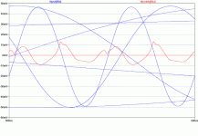
THD of voltage vs current drive of V&K output
the earlier V&K circuits are still a work in progress. There's a lot of stuff to do with stability and overload that need sorting out. But even in those aspects, it is already better than most Blameless types.
I'm trying to pin down the THD mechanisms of my topology. There appears to be only one significant source .. the output stage.
CurrentDrive.doc is my investigation and results. Sorry its a bit (??) cryptic but I write these things for myself. Please ask questions if anything is too obfuscating.
I've done this for the usual Lin topology but that shows other THD mechanisms .. particularly wonky Cob on the VAS ... may be dominant. The nice thing about V&K is that (certainly in my implementations) the other THD mechanisms are insignificant.
see eg
- #4042 on Bob's huge PA book thread
http://www.diyaudio.com/forums/solid-state/171159-bob-cordells-power-amplifier-book-405.html
.. and subsequent posts.
- #1226 on the CFA thread
http://www.diyaudio.com/forums/solid-state/240712-cfa-topology-audio-amplifiers-123.html
.. and subsequent posts.
____________________________________
The important bit in CurrenDrive.doc from near the middle where I say, "check out current driven O/P"
With the 'default' 2x58mA bias at the same o/p level, 50W 8R, Current Drive has 7.2% THD at LF and less 3.5% THD20k. ie Some cancelling taking place at HF ... and this is evident in some of my simple V&K variants too. THD is nearly all 2nd with 3rd & higher harmonics 17dB less. The THD profile is very similar to my earlier posts of simple amps with 1ppm THD
Voltage drive gives 1.8% THD. This is 12dB less than with Current Drive but you have to remember that the easiest way to arrange current drive is pure Cherry and this gives MUCH more gain at audio frequencies than the common methods for voltage drive .. plain Miller & other EVILs. The 3rd and higher order harmonics are at a higer level.
If you reduce the bias to 2x21mA (what I would want to use for a commercial amp), Voltage drive now has 3.4% THD compared to 7.2% for Current Drive .. the absolute THD difference is now only 6.5dB.
3rd now predominates in the Voltage drive case and the higher harmonics have come up. The Current drive case still has a similar THD profile.
Current Drive via pure Cherry is known to be very tolerant of bias.
The THD residual with Current drive has the characteristic 'rectified' shape which indicates a change of slope at 0V ie mismatched hfe in the 2 halves.
Here, a Bryston type arrangement might help. In production, you are likely to find devices in a single batch from good makers are quite close in hfe but this does not extend to the complementary device.
But this would convert 2nd into 3rd .. probably moot with the 1ppm THD of the full CE50d.asc amp .. though I'm sure there will be those who claim an audible advantage to mainly 2nd. I'm MUCH more concerned with STABILITY & OVERLOAD.
The Voltage drive case would have a LOT less LG in most cases and its THD residual is spikier. But not as spiky as if the comparison was made with the corresponding EF2 O/P stage. (tested in 'real life' in Jurassic times).
Attachments
Last edited:
...The important bit in CurrenDrive.doc from near the middle where I say, "check out current driven O/P"
Thanks for this, I will think it over.
But there's one comment that I noticed already.
But this would convert 2nd into 3rd
Really? Doesn't this violate Fourier?
As far as I can see, we can cancel 2nds, not convert them.
I have posted a schematic in the Bryston thread that's a bit relevant too.
Maybe follow up here, the discussion is a bit scattered.
Best wishes
David.
- Status
- Not open for further replies.
- Home
- Amplifiers
- Solid State
- Current driven OPS?