... one of the rail-to-rail OPAs.
Do you have one (or two) you favour at present?
I don't have any prejudices yet, so far my rail-to-rail ideas are based only on what I have worked out and read.
There are quite a few patents in this area, as one would expect.
US 6542032 "Extremely Linear, Hi Speed Class AB Rail to Rail Bipolar Amplifier OPS" from Texas Inst. looks like a decent start.
Then it's easy to find similar ideas, just search on patents that cite this one.
The problem is that the cost/benefits for ICs are quite different from our DIY amps.
Extra transistors are almost free on an IC and matched pairs are easy so their choices reflect this.
Whereas I would prefer to keep it simple, and only low power devices can conveniently be obtained as matched dual transistors.
Also ICs can keep transistors at accurately equal temperatures, have multiple collector transistors etc.
but always came back to the IPS - VAS - EF...
Yesterday I played around with CFA JFET self biased IPS - EF buffer to Common Base - EF buffered CE OPS.
Pretty simple and plenty of Gain but awkward to compensate.
Or perhaps it's just that it needs different techniques to what I know from VFA IPS - VAS - EF.
I will post it if anyone is interested.
Perhaps the compensation problems will drive me back to the usual solution too.
Best wishes
David
Last edited:
Yes please Guru Zan.Yesterday I played around with CFA JFET self biased IPS - EF buffer to Common Base - EF buffered CE OPS.
Pretty simple and plenty of Gain but awkward to compensate.
...
I will post it if anyone is interested.
The problem is doing good Class B (or AB) ... good bias, switching stuff off under HF overload etc.
If you're happy to have Class A, a lot more topologies are good.
You haven't commented on my suggestion of Vanderkooy & Krauel It's a simple (??) extension of present day topologies so should be amenable to your present experience of fancy compensation.
Last edited:
You haven't commented on my suggestion of Vanderkooy & Krauel It's a simple (??) extension of present day topologies so should be amenable to your present experience of fancy compensation.
Try this thread... 😉 http://www.diyaudio.com/forums/solid-state/299418-common-emitter-ops.html (Albeit my contributions refer to MOSFETs but the general architecture does not preclude BJTs).
Also worthy of mention is that the thread contains reference to the "variable" local output stage feedback employed by Isaac to minimise the difference in gain halfs and hence crossover distortion. It is an exceptionally simple and effective addition to the simple architecture later shown by Vanderkooy et al.
Yes please...
The problem is ...Class B (or AB)[/B] ...
I will post it, but Class B is the lesser problem, first problem is stability😉
You haven't commented on ...Vanderkooy & Krauel
I see the main issue as CE versus EF.
As I stated earlier in the thread, to drive a CE OPS with an IC op-amp, as V and K do, is an obvious and attractive choice.
Once that is sorted out than the floated power supply is mainly an implementation decision, certain combinations of OPS type and transistor case make more sense.
The ATC implementation, of which "Soundbloke" is an enthusiast, is one that makes sense for the lateral FETs used (Source connected to case).
The availability concerns of LatFETs make it doubtful as a future option.
Best wishes
David
Last edited:
😀Last edited by Dave Zan; Today at 11:07 AM. Reason: Preempt ATC discussion.
Putting aside the ease of using lateral MOSFETs with their sources grounded, the use of BJTs necessitates the inclusion of emitter resistors and this leads to a different thrust in my posting in this thread...
With the emitter resistors' common connected to ground and a floating supply, it is then possible without much added complexity to add local feedback around each of the output devices in separate loops - essentially measuring the emitter resistor voltages/sampling the output device currents.
The ability to then null the differences between the n and p sides as described in the previously referenced thread is an added bonus.
Furthermore, such a topology also invites "Blomley-esque" current division that allows the output devices to remain in conduction and therefore the topology to realise any potential distortion advantage of current driving the output stage.
The current division could be via an op-amp for simplicity (like Blomley) or via a matched-transistor cell that affords square law current sharing. The advantage of the latter's "complexity" is a reduction in higher frequency harmonics required from the output stage.
Of course this can all be done with the output devices referenced to the supply rails but I would suggest simplicity is a worthwhile objective here as indeed anywhere.
...the use of BJTs necessitates the inclusion of emitter resistors...
...it is then possible without much added complexity to add local feedback around each of the output devices in separate loops...
Please post a picture, not sure I correctly visualize what you have in mind.
Best wishes
David
The ability to then null the differences between the n and p sides as described in the previously referenced thread is an added bonus.
I'll throw an interesting article your way. These guys use accelerated aging (high temperature and humidity) on transistors. They find that bipolars slowly lose hFe as they age under these extreme conditions, and some transistors from the same batch age faster than others. They conclude that if you want to build high-reliability stuff for extreme environments, this is a good predictor to select the most reliable specimen.
http://www.jos.ac.cn/bdtxben/ch/reader/create_pdf.aspx?file_no=14010904
But that was a digression. I was only quoting this article for the nice hFe versus temperature equations.
hFe = constant * exp( -constant / kT )
Or check MJL1302 and MJL3281 datasheet which brags about "NPN/PNP Gain Matching within 10% from 50 mA to 5 A"...
Code:
            hFe
            25°C    100°C
MJL1302     100     200
MJL3281     100     130
Granted, I read the above values from log curves so they will not have any kind of true precision. However, if you actually use your transistor in an output stage and it heats up a little bit, goodbye hFe matching!...
so how do they "null the differences between the n and p sides" ?...
so how do they "null the differences between the n and p sides" ?...
http://www.diyaudio.com/forums/solid-state/299418-common-emitter-ops-4.html#post4900423
......Code:hFe 25°C 100°C MJL1302 100 200 MJL3281 100 130
so how do they "null the differences between the n and p sides" ?...
The issue of N and P match has been of interest lately, thanks for the observation and link.
P and N doped silicon are inevitably different so it is impossible to have perfect complements.
Manufacturer makes choices on which parameters to match and which have to be compromised as a consequence.
I expect you are correct, temperature variation will probably lead to some increased mismatches as balanced trade-offs are perturbed.
Anyone have a reference for this?
Especially for JFETs?
My interest was sparked because Linear Systems only seem to have a Spice model for the LSK170, and not its complement.
So I would like to estimate the Spice model for the LSJ74 as accurately as possible, adjust for N - P mismatch, not just make it simply complementary.
Best wishes
David
Alright 😀
I bolted a MJL1302 on a heatsink. The test jig is dead simple. Bench supply is set to deliver +/-30V.
Emitter goes to a 15R resistor to +30V.
Collector goes to -30V.
Base is connected to GND with a 100R resistor.
This makes a 2 amp (approx) CCS and the transistor dissipates 60W. A small switch allows to start it and trigger the scope, which records the voltage across the base resistor, and the supply to check if it doesn't sag.
Voltage across a resistor gives current, Ic is know, therefore we have hFe which is measured with acceptable relative precision. Don't count on absolute accuracy though, as nothing is calibrated, especially the 15R resistor, which is made up of 2x 7R5 resistors weighing about half a kilo each, that I discovered in a dumpster one day...
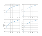
Anyway. From hFe and the datasheet, I do a heavy approximation and compute temperature. This has most likely a rather large margin for error, like +/- 50%, considering it comes from a LOG graph, so please don't look at these curves too hard. Only the hFe one can be trusted. Anyway, I plotted Vbe drift and bias drift of a theoretical output stage using this transistor with 33R emitter resistors. All 4 curves are the same data, only the scales are different.
Verdict:
- We can see two different thermal time constants here (probably die and copper slug).
- 60W thermal power during 20ms will increase hFe by 5% which is not significant.
- IMO this would matter only if the user listens VERY loud (or has super inefficient speakers)...
So, measurements are a nice thing to have! We can see there is indeed a small issue, but probably nothing to worry about.
However a circuit relying on precise matching and cancellation, and adjusted by turning a trimmer during a static measurement at 1 kHz could fall down in flames on a real signal if the cancellation rests on hFe matching between output devices...
I bolted a MJL1302 on a heatsink. The test jig is dead simple. Bench supply is set to deliver +/-30V.
Emitter goes to a 15R resistor to +30V.
Collector goes to -30V.
Base is connected to GND with a 100R resistor.
This makes a 2 amp (approx) CCS and the transistor dissipates 60W. A small switch allows to start it and trigger the scope, which records the voltage across the base resistor, and the supply to check if it doesn't sag.
Voltage across a resistor gives current, Ic is know, therefore we have hFe which is measured with acceptable relative precision. Don't count on absolute accuracy though, as nothing is calibrated, especially the 15R resistor, which is made up of 2x 7R5 resistors weighing about half a kilo each, that I discovered in a dumpster one day...
Anyway. From hFe and the datasheet, I do a heavy approximation and compute temperature. This has most likely a rather large margin for error, like +/- 50%, considering it comes from a LOG graph, so please don't look at these curves too hard. Only the hFe one can be trusted. Anyway, I plotted Vbe drift and bias drift of a theoretical output stage using this transistor with 33R emitter resistors. All 4 curves are the same data, only the scales are different.
Verdict:
- We can see two different thermal time constants here (probably die and copper slug).
- 60W thermal power during 20ms will increase hFe by 5% which is not significant.
- IMO this would matter only if the user listens VERY loud (or has super inefficient speakers)...
So, measurements are a nice thing to have! We can see there is indeed a small issue, but probably nothing to worry about.
However a circuit relying on precise matching and cancellation, and adjusted by turning a trimmer during a static measurement at 1 kHz could fall down in flames on a real signal if the cancellation rests on hFe matching between output devices...
Attachments
Last edited:
...I bolted a MJL1302 on a heatsink...
Do you have an MJL3201 complement?
It would be instructive to see if they both have a similar temperature coefficient for the hFE and Vbe.
Best wishes
David
3281/1302 are rather complementary, based on both the datasheet and my experience, however it will be interesting to see the measurement exercise results in the same conditions anyway 😉
A few thoughts.
When we say "matched" - we normally don't expect the parameters to be exactly the same, especially in a complementary pair - they never will. For me, if we stay within some +/-20% threshold - we're fine.
Example (hFE): 150 vs 50 = unmatched; 150 vs 180 = matched pretty well.
OK - what hFE drift means to us. Let's take a simple EF OPS as an example.
EF is basically a voltage follower. Now it all comes to impedances 🙂
We want the EF stage (with certain input impedance) to replicate its input signal at its output, driving a much lower impedance of the load. OK, that's the way it works, however we have one (at least 😉) unwanted thing here - the base current Ib. As collector current changes all the time, following the waveform, the base current changes proportionally, modulating the input impedance of our EF stage. Now, if hFE is different for the N and P halves of the push-pull arrangement, plus it drifts somewhat asymmetrically - that's the reason why we see the distortion increased - asymmetric modulation of the input impedance of our EF stage (influencing the previous stage - VAS - performance).
So, what we need to do to reduce the distortion - is to decrease the influence of OPS impedance modulation on VAS performance. There are many ways of doing this - normally, particular engineering solution includes some combination of them. For example, a good result is achieved by loading the driver stage by CCSs (dynamic load), setting the constant current high enough, resulting in significant reduction of the output transistors' base current modulation influence. In this case, the fact, that hFE of the output pair drifts with some asymmetry as they warm up, does not "scare" us any more. Input impedance of the driver stage stays constant enough. Another straight forward solution - one more follower in front of the drivers - it may be complementary or single sided with CCS load, with slightly different effects in place.
No doubt, this is not the only distortion mechanism in place, but a rather significant one. For me, a well-engineered circuit is the one, where hFE drift within 20...50% does not noticeably influence the performance.
Cheers,
Valery
Attachments
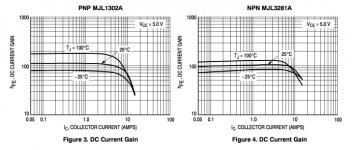
3281/1302 are rather complementary, based on both the datasheet and my experience...
Your picture illustrates the point made earlier, that PNP and NPN could be well matched at 25 C but would be mismatched at, say 100 C.
I am curious to know if this is real or just a sloppy plot.
Your explanation of the effect of hFE mismatch seems a useful way to look at the problem.
Best wishes
David
I have the NPN in stock. Before testing it, I upgraded the jig and software. See here 😀
http://www.diyaudio.com/forums/solid-state/303479-thermal-modeling-transistors.html
http://www.diyaudio.com/forums/solid-state/303479-thermal-modeling-transistors.html
I have the NPN in stock...
Nice effort, haven't really checked it yet but it looks like some difference between the PNP and NPN temperature coefficients is real.
Anyone know the reason for this?
Otherwise I have to study more semiconductor physics😉
Best wishes
David
Last edited:
Don't forget Black's initial reason for 'inventing' feedback was to make the circuit immune to the vagaries of component & device drift / variation.3281/1302 are rather complementary, based on both the datasheet and my experience, however it will be interesting to see the measurement exercise results ...
.... loadsa good stuff including
.... For me, a well-engineered circuit is the one, where hFE drift within 20...50% does not noticeably influence the performance.
I don't think we should rely on any matching beyond what you can sensibly tell a Purchasing Manager ... eg "BC550C : ie hfe more than 420"
Black, Nyquist & Bode
http://www.ieeecss.org/CSM/library/1993/aug1993/w04-HistoricalPerspectives.pdf
Guru Zan, this is off-topic but I'm sure you won't mind. I traces the links between these 3 men for which we should be eternally grateful.
Bell Labs was THE powerhouse of innovation in da old days.
I wonder if there is anything like it today. Please don't make me laugh by mentioning Apple etc.
And sadly, this may soon become just a fable if Trump's Min. of Truth (dedicated to Alternative Facts & Improving History) has its way.
Vanderkooy & Krauel
Guru Zan,
I'm posting my attempt at Vanderkooy & Krauel.
The topology is/was my Jurassic favourite for certain fail-safe behaviour which may not be needed with V&K
This version has <10ppm @ 20kHz 50W 8R with only 3 gain stages (4 if you include IPS) .. at least in simworld
I'm sure you'll complain about the small margins but its from a quick look at 2R stability. The original hacked circuit had stabilty problems until I sorted out more sensible IPS & VAS currents for these +/-15V stages.
aI'm using Cherry's favourite 'Zobel' for which I still haven't found the worst case loads. (for the usual 8R+100n before the 2uH/8R networks, its small 1-10n capacitance) Maybe its the least fussy.
You'll like the way the stages appear like a block diagram for an IEEE TRans paper on stability 😀
They also form nice NDFLs .. eg the output & driver are a 2nd order differentiator which becomes 1st order with C1&7
Though there's a lot more work to do, I really like this topology. eg it can be easily converted to a Current Drive amp for speaker testing.
Still not sure if this is the ideal topology for V&K .. or if going back to a Blameless-type is better.
Attachments
Last edited:
...I'm sure you'll complain about the small ...
I would never complain, I would, however be worried.
30 degrees PM is too scary for me.
If you can land the phase peak directly on top of the ULGF, that would leave you closer to 60.
Have you tried added stray capacitance on the power supply to see what it does to stability?
That is one of my main concerns for this sort of circuit.
Thanks for the ASC, I will experiment and see what I find.
Best wishes
David
I am not convinced by the whole NDFL concept, despite my respect for Dr Cherry.They also form nice NDFLs
Last edited:
Ok, a few more ideas,partly as reminder to me and discussion points.
The very small PM means the Loop Gain must be accurately estimated.
The position you have looks essentially correct but Tian probe is theoretically not quite correct.
Usually this makes no practical difference but I am not sure about this case because the feedback loops are interconnected.
Why do my friends always do the most complicated compensation😉
I recently found some nice, heavy duty (500W), fairly complementary VFETs.
I mentioned to Toni that they looked ideal for an amp, and he was incredibly quick to jump in.
So I did LTSpice VDMOS models with the latest sub-threshold parameters.
Toni did his usual excellent build, it's in his thread, summary is that the models worked well and so do the transistors.
They look ideal for a CE/CS amp, the ~4 V threshold ceases to be a problem and becomes actually useful.
I can send you the preliminary models if you want, not ready to release them publicly until I have checked them some more.
Best wishes
David
- Status
- Not open for further replies.
- Home
- Amplifiers
- Solid State
- Current driven OPS?