
Hi, Calvin,
Current conveyor circuits have drawbacks as well. For example, unless such a circuit utilizes some local or global feedback loop to attain low distortion I/V conversion, the conveyor bias current needs to be quite high relative to the peak signal current, maybe by a factor of ten. This also places significant and broadband dynamic current demands upon the local regulators supplying the current conveyor. In addition, some of the best current output DAC chips (PCM179x and AD1955) need to source or sink their own D.C. bias currents in to a current conveyor, which could severely upset the circuit operating symmetry if not offset by some matched complementary secondary current source or sink.
Those implementation concerns keep pushing me away from current conveyors (despite my appreciation for their conceptual logic) and back to an low value passive resistor I/V, followed by simple passive low-pass filtering, followed by active open-loop voltage amplification.
I am sorry Ken, but I have to disagree with you.
What you said is true for low output impedance DAC chips like for example the trendy ES9018, but not for a high output impedance DAC chip like the PCM1794.
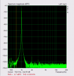
This picture are the distortion of a single-ended common base like the one Calvin use, connected to a single output of a PCM1794 at -1dB .
this is a very simple circuit than only uses 2 npn transistors and 2 jfet as ccs, the current that passes through the circuit is only 15mA.
The distortion is only 0.00018%
There is no problem with the d.c. bias as this is a single-ended circuit and it has a output capacitor.
Even such a simple current conveyor can outperform the 0.0004% distortion from the PCM1794 datasheet.
These last months I have test a lot of I/V converters, and I can say that is very easy to have very low distortion out of a PCM1794 without using feedback .
But ofcourse distortion is not everything , and the current conveyor that I end up to chose, is a folded cascode with the famous 2sk170 and 2sj74 the distortion at -1db is 0.003% pure 2º harmonic, the sound is just amazing, and I am enjoying my music like never before.
😎
Attachments
Last edited:
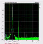
This pictures are from the same current conveyor as the one from the post above, and also with -1db, but this time with a resistor in parallel with the output of the dac chip, to simulate a DAC with lower output impedance, the first is with 1000R and the second 220R the distortion is much worst and even with a 10K resistor the distortion is now 0.0015%
As we can see from this, simple solutions like single-ended common base are not easy to implement in chips like the ES9018 that has a output impedance lower than 200R.
As we can see from this, simple solutions like single-ended common base are not easy to implement in chips like the ES9018 that has a output impedance lower than 200R.
Attachments

A few years back, I tried this one, based on a suggestion of Cauhtemoc from here.
It worked well but there was no magic improvement over the opa1632, quite the contrary.
That circuit is the perfect example of unnecessary complexity. 🙄
I tried zero field input transformer I/V circuits as well, but the transformer always adds substantial distortion.
I am sad to hear that, You were so confident in the circuit... I guess it can happen when one is stepping new territories.
Calvin , thanks very much for your answer 🙂 , I have download the paper that you suggested, It seems interesting , but only had time for a brief look, I will see it better.
Have also to take a second look (audition) to the single-ended common base circuit 😉 .
Tchau.
Have also to take a second look (audition) to the single-ended common base circuit 😉 .
Tchau.
Last edited:
Hi,
Yes, every circuit has inevitably drawbacks and requires compromising.
And also yes, that in principle it is good, THD-wise, to keep the percentage of signal swing as part of Bias small.
In qusp's thread where a single MOSFET were used in a common gate arrangement, they got impressively low THD values running the FET on 75V/300mA (afairc).
The common base circuit I used ran on ~10mA and +-15V, fed by the -3.5mA+-2mA of a PCM1795/96. A PCM1794 required slightly more bias, but still <<20mA. All values low enough to allow for SOT23 or similar SMD casings.
The THD performance is admittedly a bit sensitive to bias settings, and also to the DACs output impedance. For lowest THD the source impedance should be high.
I kindly disagree about the current conveyor beeing inferior with DACs featuring an offset current like the AD1955 or TI's PCM179x series.
With symmetrical complementary current conveyors one needed a dedicated current source/sink to cancel the DACs centre current.
But this is not the case when You go single ended as with the 4 principle examples shown before (see the current labels, e.g I1=Idac+Iq1).
First sims I did yestday showed that THD decreased to <-100dB when Q1 of the common base circuit were replaced by a CFP. (PCM1795/96, 0dBfs, 1kHz, 2Vrms output, +-15V supplies, ~11mA at idle, Zin<1Ohm with sufficient bandwidth).
I don't see any practical advantage going more complex from here, apart from adding a buffer of course.
jauu
Calvin
@Calvin: CFP sim very nicely... in real life, it's worth checking for unstability at high frequencies. I wouldn't have gone for the "too complex circuit" otherwise (which btw is not that complicated; cascodes and transistors used as diodes just make it look complex).
I am sorry Ken, but I have to disagree with you.
What you said is true for low output impedance DAC chips like for example the trendy ES9018, but not for a high output impedance DAC chip like the PCM1794.
This picture are the distortion of a single-ended common base like the one Calvin use, connected to a single output of a PCM1794 at -1dB .
this is a very simple circuit than only uses 2 npn transistors and 2 jfet as ccs, the current that passes through the circuit is only 15mA.
The distortion is only 0.00018%
There is no problem with the d.c. bias as this is a single-ended circuit and it has a output capacitor.
Even such a simple current conveyor can outperform the 0.0004% distortion from the PCM1794 datasheet.
These last months I have test a lot of I/V converters, and I can say that is very easy to have very low distortion out of a PCM1794 without using feedback .
But ofcourse distortion is not everything , and the current conveyor that I end up to chose, is a folded cascode with the famous 2sk170 and 2sj74 the distortion at -1db is 0.003% pure 2º harmonic, the sound is just amazing, and I am enjoying my music like never before.
😎
Hi, Sergio,
Please don't be sorry for disagreeing. I'm always happy to learn of a better way to accomplish something. That's what makes being a member here most interesting. 🙂
Regarding your two transistor I/V, does it utilize a feedback loop to obtain such low distortion while running with such relatively low bias currents? I've never been able to get low open loop distortion utilizing only two transistors and at such low bias currents, including with circuits using the K170 and J74 audio JFETs in a cascode.
I kindly disagree about the current conveyor beeing inferior with DACs featuring an offset current like the AD1955 or TI's PCM179x series.
With symmetrical complementary current conveyors one needed a dedicated current source/sink to cancel the DACs centre current.
But this is not the case when You go single ended as with the 4 principle examples shown before (see the current labels, e.g I1=Idac+Iq1).
First sims I did yestday showed that THD decreased to <-100dB when Q1 of the common base circuit were replaced by a CFP. (PCM1795/96, 0dBfs, 1kHz, 2Vrms output, +-15V supplies, ~11mA at idle, Zin<1Ohm with sufficient bandwidth).
I don't see any practical advantage going more complex from here, apart from adding a buffer of course.
jauu
Calvin
Some folks would say that using a coupling capacitor is just as evil as using global feedback. I'm not necessarily one of them, but there are limits to every approach.
I am sad to hear that, You were so confident in the circuit... I guess it can happen when one is stepping new territories.
Well, I should qualify what I said because I did not actually connect it to a DAC, so I didn't have a proper balanced current source to drive the transformer with. I don't actually remember what I used, but it was probably less than ideal. It may still work well, I don't know, but I do know that it's robust and simple at the same time. Those are always valuable qualities in my mind.
I do have a question however. Does anyone know if the stair step waveform on the outputs of the Iout+ and Iout- pins of a PCM1794a is a common mode or differential mode signal?
Hi, Sergio,
Please don't be sorry for disagreeing. I'm always happy to learn of a better way to accomplish something. That's what makes being a member here most interesting. 🙂
Regarding your two transistor I/V, does it utilize a feedback loop to obtain such low distortion while running with such relatively low bias currents? I've never been able to get low open loop distortion utilizing only two transistors and at such low bias currents, including with circuits using the K170 and J74 audio JFETs in a cascode.
no, does not use a feedback loop , I have already sent the schematic for your email. check it.
Hi,
Cascoding/stacking current sources and current mirrors is imho alot more prone to instabilities if the transistors are not carefully matched, which requires more effort or cost. The common base, or CFPed -common base are easier and less demanding in this regard.
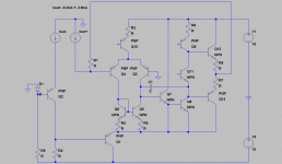
BTW. similar to Sergio I don´t understand the complexity of Your circuit. What are Q9/Q17 intended for?
Do Q10/11 really improve signal quality/THD here?
The current through the ´cancellation transistor´ Q7 needs to be constant.
A simple resistor or a simple CCS may suffice here. Why do You employ a current mirror? Compare Your circuit to the SE-Bakuun of #17. Adding a ccs towards Vnegative and connect Riv to gnd instead and You see a simplified NPN-version of Your circuit. Maybe I´ll CFP it and sim that for comparison too 😉
The DC-blocking Cap and a global feedback loop serve very different tasks in first case. And one should not forget that a DC-servo loop usually requires more devices, active and passive. In fact using a servo typically even means more Caps within the signal path. 😛
jauu
Calvin
Yes that issue should be checked. The counter measure to that would be a small compensation cap. Easy to implement.checking for unstability at high frequencies
Cascoding/stacking current sources and current mirrors is imho alot more prone to instabilities if the transistors are not carefully matched, which requires more effort or cost. The common base, or CFPed -common base are easier and less demanding in this regard.
BTW. similar to Sergio I don´t understand the complexity of Your circuit. What are Q9/Q17 intended for?
Do Q10/11 really improve signal quality/THD here?
The current through the ´cancellation transistor´ Q7 needs to be constant.
A simple resistor or a simple CCS may suffice here. Why do You employ a current mirror? Compare Your circuit to the SE-Bakuun of #17. Adding a ccs towards Vnegative and connect Riv to gnd instead and You see a simplified NPN-version of Your circuit. Maybe I´ll CFP it and sim that for comparison too 😉
well, one could use local feedback and additional circuitry/level translators to omit with both 😉Some folks would say that using a coupling capacitor is just as evil as using global feedback.
The DC-blocking Cap and a global feedback loop serve very different tasks in first case. And one should not forget that a DC-servo loop usually requires more devices, active and passive. In fact using a servo typically even means more Caps within the signal path. 😛
jauu
Calvin
no, does not use a feedback loop , I have already sent the schematic for your email. check it.
Hi, Sergio,
For some reason, that schematic hasn't arrived. Please try resending it. Thanks.
Hi,
BTW. similar to Sergio I don´t understand the complexity of Your circuit. What are Q9/Q17 intended for?
Do Q10/11 really improve signal quality/THD here?
The current through the ´cancellation transistor´ Q7 needs to be constant.
A simple resistor or a simple CCS may suffice here. Why do You employ a current mirror? Compare Your circuit to the SE-Bakuun of #17. Adding a ccs towards Vnegative and connect Riv to gnd instead and You see a simplified NPN-version of Your circuit. Maybe I´ll CFP it and sim that for comparison too 😉
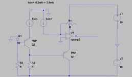
I think i have made a bad choice of words, I think the circuit is to complex for the PCM1794 , but nonetheless it is a very smart circuit, and can be very usefull for low impedance dac chips. why ?
well , the most interesting caracteristic of the circuit is the use of a error correction mechanism , the current mirror formed by Q5/Q6 will mirror the current that passes through Q17/Q8 in Q7/Q9 , so Q7/Q9 Vbe variation will compensate the Vbe variation on Q17/Q8, this will make the input impedance very low.
ofcourse the error correction loop will work without the q9/q17 transistors, but they form a circuit like the wilson current source that has a feedback loop that also help to lower the input impedance of the I/V converter.
(Q10 / Q11 / Q12 ) and ( Q1 Q2 Q3 ) only serves to make the Vce of the current mirrors low , to increase temperature stability.
The distortion mechanisms than one has to deal in the case of the PCM1794 is the early voltage distortion and the none linearity parasitic capacitances, and that circuit do a poor job in that department.
By my experience in error correction loops, I am almost certain that it needs compensation in the EC loop.
Hope I was clear enough, this time 😉
Hi,
simmed the circuit from #18 for +-2mApp -3.5mAdc (PCM1795/96) and 2Vrms fullscale output.
THD@1kHz: 0.0026% -91.7dB
noise(20Hz-20kHz): 12.61µVrms -98dBV
Zin: 2.2mOhm, rising >100kHz
Serious oscillations even with Civ. Not useable wthout compensation as in schem.
As with all aktive loads (be it CCS, folded cascode or CM) noise is quite high.
Output nulling reacts quite sensitive on trimming.
Zin is very low and linear up to >10MHz
The current conveyor transistors need to take the DACs centre current - run on high idle currents.
A complementary circuit would place the burdon on the current source transistors instead.
For the same conditions the simple CFP current conveyor sims far better.
It offers lower THD, lower noise, lower part number count/effort/cost and lower power consumption.
No difficulty in dialling into dc-bias and input-null points.
Merely a slight overshoot than tendency of oscillation.
Zin is higher but linear and low enough to not cause trouble with highimpedance output DACs.
JFET CCS provides for lowest noise of all CCS here.
jauu
Calvin
Attachments


Last edited:
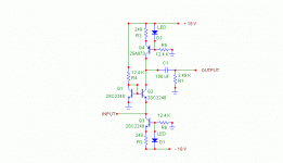
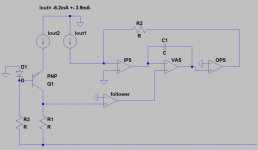
how is this circuit.
OPA is PNP or PchFET IPS ,and miller compensation VAS, 4558 or similar architecture one.
common base IVC 's output voltage swing is in-phase to OPA output.
bootstrapping OPA's -rail with it make the OPA's VAS like "differential receiver".
it helps the OPA's slew rate.
OPA is PNP or PchFET IPS ,and miller compensation VAS, 4558 or similar architecture one.
common base IVC 's output voltage swing is in-phase to OPA output.
bootstrapping OPA's -rail with it make the OPA's VAS like "differential receiver".
it helps the OPA's slew rate.
Attachments
how is this circuit.
OPA is PNP or PchFET IPS ,and miller compensation VAS, 4558 or similar architecture one.
common base IVC 's output voltage swing is in-phase to OPA output.
bootstrapping OPA's -rail with it make the OPA's VAS like "differential receiver".
it helps the OPA's slew rate.
Bootstrapped op-amp circuits are interesting. One just needs to be careful about properly observing the op-amp's common-mode voltage swing limits.
- Status
- Not open for further replies.
- Home
- Source & Line
- Digital Line Level
- Current differential to voltage line level from PCM1794 et al