Hi all!
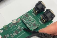
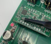
It has been my intention for some time to make a multiway digital crossover with minimal parts. I have designed a tiny little DIP-24 board featuring two onboard CS43131 DACs, MCU, regulators and level shifters. The schematic pretty much follows the Cirrus reference designs.
The CS43131 has one first-order IIR and three second-order IIR filters that should allow for "simple" crossovers and perhaps an EQ.
During boot the MCU sets up each CS43131 into a default i2s 24/96 mono mode expecting a 19.2Mhz clock on pins MC1/MC2. The master clock is then derived using the internal DAC PLL for whatever frequency setting is required.
Shortly after boot the external level i2c (3.3v) bridge becomes available for further configuration. I hope to develop a simple Arudio lib to edit the clock setup, audio source and output filters.
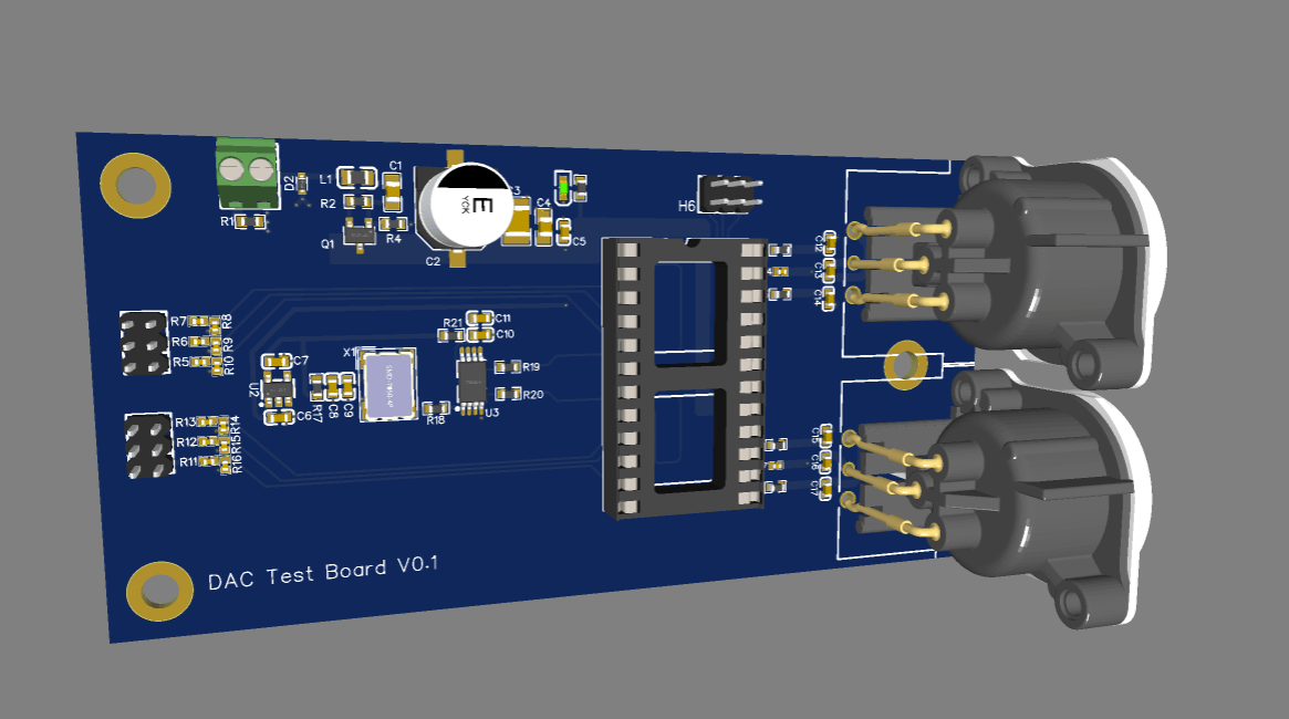
I am expecting the delivery today of a test board featuring a SiT8208AI 19.2Mhz clock and XLR outputs.
More to follow!
CS43131 - Dual Mono Configuration
https://www.cirrus.com/products/cs43131/
5x Toshiba TCR3RM Regulators ~ 5 μVrms
https://toshiba.semicon-storage.com/info/docget.jsp?did=69842&prodName=TCR3RM18A
Level shifters
to 1.8v for i2c, i2s, dsd clocks and data
Boot and config MCU
Cypress Semiconductor
Last edited:
DHL delivery!
The part for the DIP-24 "socket" is wrong. Note to self. 3D models provided with software are not always right!
clock source
SiT8208AI-83-33E-19.200000Y
https://www.sitime.com/datasheet/SiT8208
clock buffer
CDCLVC1102PWR
https://www.ti.com/lit/ds/symlink/cdclvc1102.pdf
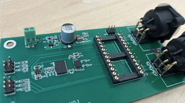
The part for the DIP-24 "socket" is wrong. Note to self. 3D models provided with software are not always right!
clock source
SiT8208AI-83-33E-19.200000Y
https://www.sitime.com/datasheet/SiT8208
clock buffer
CDCLVC1102PWR
https://www.ti.com/lit/ds/symlink/cdclvc1102.pdf
Last edited:
The dual mono DIP board is not a great departure from the CDB43131 ref design -just a change to smaller parts.
FXLA0104QFX level shifters
https://www.onsemi.com/pdf/datasheet/fxla0104-d.pdf
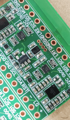
CY8C4045FNI-DS400T for boot up settings that can be programmed using the little 1mm pitch header next to it.
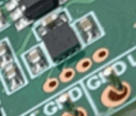
This little Cortex-MO part has a 3.3v tolerant i2c port (SCB0) for external communication. I'm using SCB1 at vddio level (1.8v) to connect to the two CS43131.
FXLA0104QFX level shifters
https://www.onsemi.com/pdf/datasheet/fxla0104-d.pdf
CY8C4045FNI-DS400T for boot up settings that can be programmed using the little 1mm pitch header next to it.
This little Cortex-MO part has a 3.3v tolerant i2c port (SCB0) for external communication. I'm using SCB1 at vddio level (1.8v) to connect to the two CS43131.
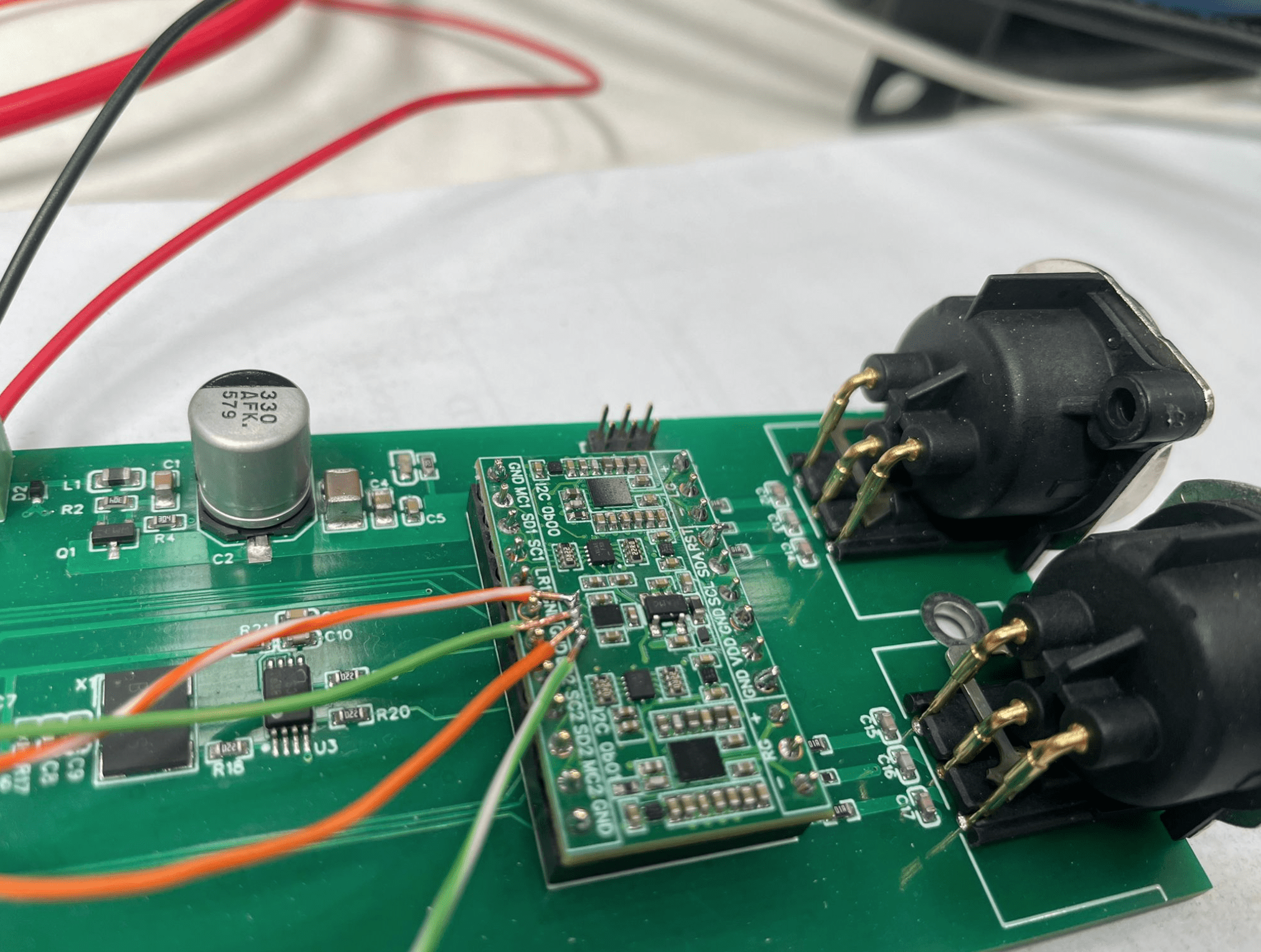
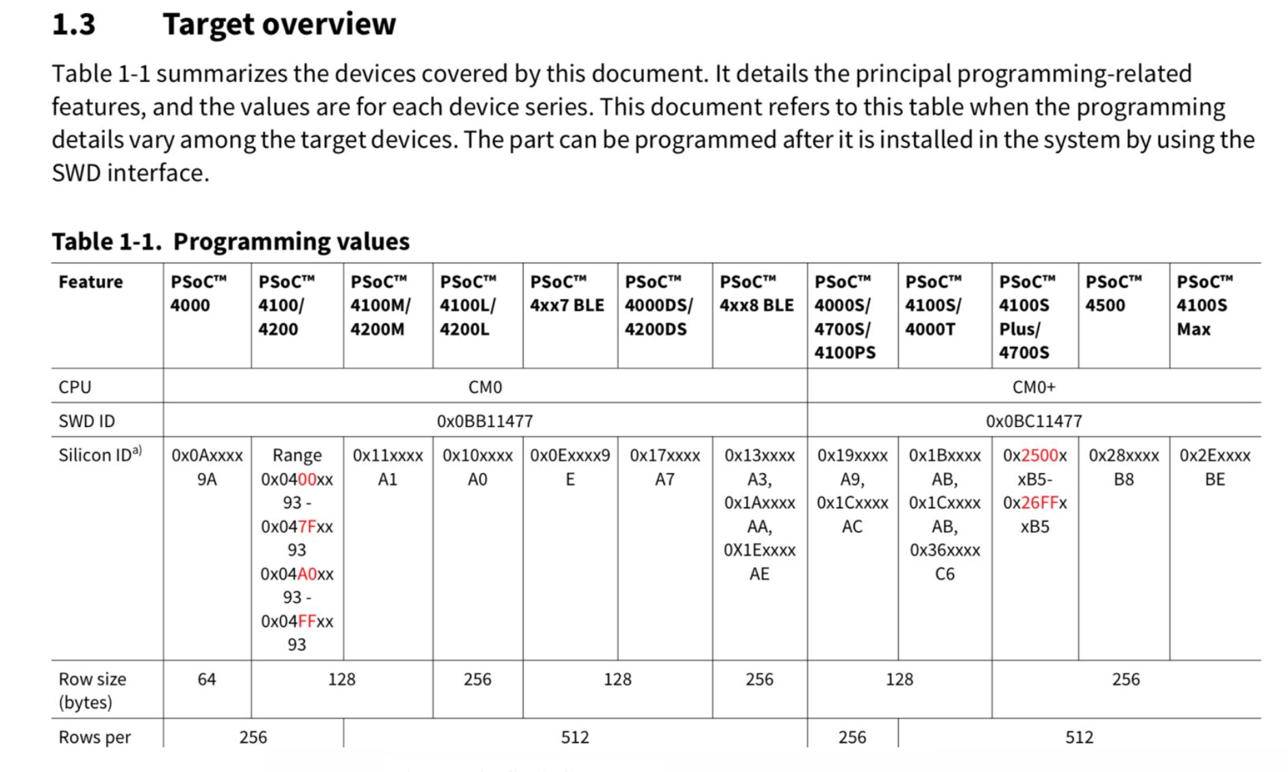
Some diagnostics required! The PSOC programmer is returning a fault saying that "ID 19_A0_13_A4" is unsupported. Perhaps I have a sticky bit somewhere. The CY8C4045FNI-DS400 is part of the 4000DS family so should be "ID 17_xx_xx_A7"
Fault could be
1). poor circuit
2). incomplete software at Cypress for this silicon / revision
3). bad silicon
4). programming cable too long causing bit errors

Fault could be
1). poor circuit
2). incomplete software at Cypress for this silicon / revision
3). bad silicon
4). programming cable too long causing bit errors
Last edited:
Very confused.
PSoC Creator target selector suggests CY8C4045FNI-DS400 family is 4000DS with ID 0x19xxxxA9
The PSoC 4 series TRM "1.3 Target Overview" says the 4000DS should be 0x17xxxxA7.
PSoC Creator target selector suggests CY8C4045FNI-DS400 family is 4000DS with ID 0x19xxxxA9
The PSoC 4 series TRM "1.3 Target Overview" says the 4000DS should be 0x17xxxxA7.
Reworked for QFN parts and switched to LPC804UKAZ for boot time config.
Much less symmetry in the layout. Ohwell.
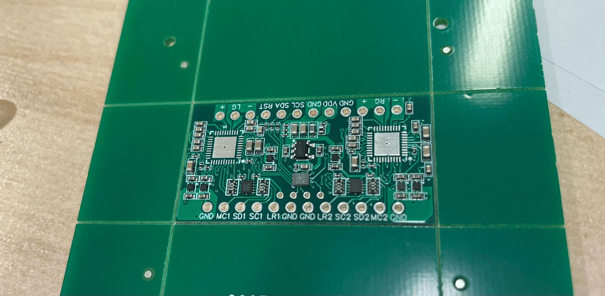
Much less symmetry in the layout. Ohwell.
Last edited:
Should be able to pre program LPC804 and test crossovers for i2s/dsd to 2-way amps / speakers. Hopefully provide an app to change via i2c.
Last edited:
Finally got around to programming the LPC804. I have enough I/O to make a 4 bit settings dip switch. Might do that next revision. Otherwise there is i2c pass through by address.
Last edited:
Hello, I am lucky to see your post, I am very interested, want to make one to play, can you share your circuit diagram as a reference design
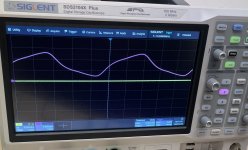
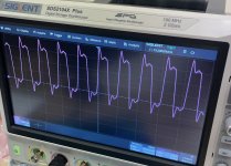
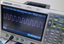
Hi there are to much ground bounces and peek that extend Vpower.Found the correct settings.
Before and after the 3.3 to 1.8 level translator (FLXA0104)
Output from CDCLVC1102
View attachment 1170010
Input into CS43131
View attachment 1170007
View attachment 1170008
In booth sases in and out. That is introducing huge amount of digital noise in the system, and "polluting" even mid range of audio BW...
.
Try to trim for signal integrity every line. It will be different because of the diff Fr.
That is to add just one R before logic gate. Usually that is 33 to 47 ohms.
But it coukd be higher value. And it should be determinated with scope that You alredy have.
Probably it has some R in the line path but from lower value...
That will be easy to exchange vith some higher until spikes flatten down.
But there are the chances that there are no R in PCB prior to the input of logic, then manage with some other way... ;(
cheers
.
PS try to find simple data about values of LO and HI for each standard. Because You can "round" the suares even more, BUT not out of the stadard range...
- Home
- Source & Line
- Digital Line Level
- CS43131 ( DSD & i2S ) - A Dual Mono DAC on a DIP-24
