Look into the attachment. I found this somewhere on the Internet. Don't remember even where. This is the part of the whole DAC circuit based on 8420 and 43122. It's only output stage for 43122. What do you think ? Does anybody know that circuit ? I'm not quite familiar with that I assume R+ and R- are inputs and right under mosfets are outputs. Any comments ?

Thanks
Thanks
Attachments
This schematic begins here in the digital forum, do a search using "cheap 24/96 dac" as keywords. However, I think a better output stage is using tubes, such as
http://members.brabant.chello.nl/~m.heijligers/DAChtml/dactop.htm
or use subminiature tubes. Click on the 6021W Tube Dac link below:
http://amps.zugster.net/projects/sub-mini/
http://members.brabant.chello.nl/~m.heijligers/DAChtml/dactop.htm
or use subminiature tubes. Click on the 6021W Tube Dac link below:
http://amps.zugster.net/projects/sub-mini/
dac output
Although the schematic looks all right I would prefer a much higher supply voltage.
You may find an alternative in our MP-DAC at www.audio.nl
John
Although the schematic looks all right I would prefer a much higher supply voltage.
You may find an alternative in our MP-DAC at www.audio.nl
John
output
johnrtd
About what level of voltage are we talking here ? Do I need to do any modifications to the circuit then. My dacs output stages are mostly built on opamps but it's time to try something else/better. Did I correctly describe outputs and inputs in my first post. ? 🙁
johnrtd
About what level of voltage are we talking here ? Do I need to do any modifications to the circuit then. My dacs output stages are mostly built on opamps but it's time to try something else/better. Did I correctly describe outputs and inputs in my first post. ? 🙁
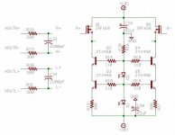
This is my schematic. You may freely reproduce it with attribution to me.
My drawing abilities are extremely bad of course, depite years of formal training. The terminals labelled AOUT[RL][+-] are the pins on the 43122 chip itself. R29-R31 and C33-C34 form a low-pass filter. The terminals labelled [RL][+-] are the resultant output voltages.
The circuit on the right is simply a MOSFET line driver with an active current source load. It presents a very easy load for the DAC and can drive difficult loads at the other end. Q2-Q5 are the cascoded current sources. Adjust R13 and R17 for more or less idle current. The rail voltage can be up to ± 24V, or even higher if you wish.
Connect your output wires to the MOSFET source pins.
You'll probably want to read this thread:
Cheap 24/96 DAC, Revision B.
- Status
- Not open for further replies.