
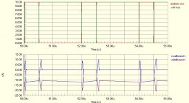
It looks like the reverse recovery transient and it corresponds with the off time of about 100ns plus the reverse recovery time of 100ns in the IRF530 datasheet.
Hi, BWRX,
Thanks for the input 😀 Is there any trick to eliminate this cross conduction? I tried with IRF540-9540 and they are worse.
Why this cross conduction don't show up if I make on-time 1uS (50% of 2uS), and become worse with smaller dead time?
Thanks for the input 😀 Is there any trick to eliminate this cross conduction? I tried with IRF540-9540 and they are worse.
Why this cross conduction don't show up if I make on-time 1uS (50% of 2uS), and become worse with smaller dead time?
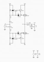
Try adding a 200ohm resistor in series with D2 and an RC snubber (R=10ohms, C=0.22uF) between VDD and SW. That helps get rid of some of the cross conduction but not all of it. I can post the switchercad files of the simulation I cobbled together in a little bit.
Untamed Goliath posing problems
Hi David,
R1,R2 should be atleast 1K or even less to speedup turn-off and insert the Rg as said by BWRX to slow turn-On time.
Trr=100nS is enough fast if the SWF=300KHZ even, in Class-D operation
Kanwar
Hi David,
R1,R2 should be atleast 1K or even less to speedup turn-off and insert the Rg as said by BWRX to slow turn-On time.
Trr=100nS is enough fast if the SWF=300KHZ even, in Class-D operation
Kanwar
There is a good paper on body dioda Qrr, IR AN-967.
It's really a problem in high speed switching. This cross conduction won't show up in idle, but appears in modulated/loaded condition.
I wonder how Fumac get away with this in Mhz modulation, this Trr will be very big compared to the Mhz timing period.
BWRX, Kanwar, I will try to sim your suggestions, thanks.
Hi, BWRX, Kanwar,
I've simmed both your suggestions. Unfortunately, none can help.
R//with back diode can only delay about 10'ns, that's all.
Is there any other "passive trick" that can delay up to 100ns?
I've simmed both your suggestions. Unfortunately, none can help.
R//with back diode can only delay about 10'ns, that's all.
Is there any other "passive trick" that can delay up to 100ns?
You cannot push your circuit harder...om...😀 your circuit seems as a lazy circuit 🙂 Don't expect too much.
Hi, Kartino,
You're right, it is a simple and cheap classD output 😀. But the more I study the cause, I found out that this cross-conduction will happen to all classD output topology, since it is caused by body dioda of a mosfet, not due to a certain topology. If you use adjustable "on" dead time for upper and lower mosfet, this Trr can be pursued (not to happen) in expense of wider dead time (=more distortion).
In 100's of khz switching, this body dioda reverse recovery is really a problem. It makes cross conduction of 10's of ampere (although the time is very narrow, but enough to heat up the mosfet). This will not show up at idle, you have to burden the output stage to make it show up. I think the heat caused by this body dioda cross conduction is higher than Rds heat.
The only remedy so far is to choose a better mosfet, with low Trr and low Qrr (like IRF540Z), or choosing the difficult way, bypassing internal body dioda and use external 30ns dioda.
bypassing body dioda
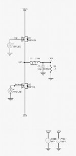
Reading SMALA amps (Steven's URL), I saw this interesting picture.
Imagine this is an output stage of classD amp. There will be C // with Rload (to complete LC filter).
To bypass body diode, it is possible with this configuration. It saves 2 schottky series diode.
But it needs 2 inductors.
IC7+D1 works independently towards IC8+D2. We can pick 30nS diodes for D1 and D2, so the internal body diode of mosfets are not used.
My question is about the inductors.
Is it possible to use only 1 core, bifiliar winding for making both L1 and L2, or these needs independent cores?
Attachments
Hi, Kanwar,
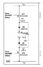
Yes, it is BCA output stage. I guess the answer to my question is "No", BCA needs independent cores (cannot be on one core, bifiliar, made a transformer that way).
So, the body dioda is naturally unused in BCA output stage.
Anybody has tried this output stage with ordinary loop, the one used for half bridge (not BCA loop)?
- Status
- Not open for further replies.
- Home
- Amplifiers
- Class D
- Cross Conduction