I created the schematic for the front end of a very simple amp for the purpose of practicing hand routing PCBs. I doubt I will etch this.
Please critique my attempt. My main trouble is that I wanted the rails to be in close proximity, and more "deliberate" looking. I probably would have fattened up the rail traces if I had been happy with their placement. I think the ground plane is ugly too.
Any thoughts?
Please critique my attempt. My main trouble is that I wanted the rails to be in close proximity, and more "deliberate" looking. I probably would have fattened up the rail traces if I had been happy with their placement. I think the ground plane is ugly too.
Any thoughts?
Attachments
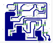
I also just realized that in some cases the ground plane obscures the components. This happened somehow when I printed to the .pdf, as it looks right in the Eagle editor. Doesn't really matter in the end, as I would only print the copper for home etching.
Eh, where does one start?
A few hints:
1) The PCB component positions may not (and usually do not) correspond to their positions in the schematic drawing for optimum placement. This is because actual components sizes vary while simbols on schematics are always the same. Also actual components heat up and sometime sneed space to cool adequately or must be thermally coupled (close to each other). Finally, actual component pinouts may not even resemble the positions on a schematic drawing. In other words, the schematic drawing shows how components must be connected, positions are subject to a whole different set of rules.
2) Think small, short, close. The longer the tracks, the more problems you are asking for - even in simple designs. Schematics show ideal wires, PCBs are not symbolic representations of the real world, rather THE real world.
3) Expect to go through several iterations on placement until you find something that's OK and even more fine tuning to get it good.
4) Use ACTUAL component sizes, which means you should on occasion define your own component footprints and outlines not just use the ones from the library. From the generallook of things you are using Eagle. Some of it's components are defined criminally badly. Think out of the box, mounting a TO-92 transistor at a 45 deg angle will give you 3 out of four points in a rectangle which is much easyer to put on a grid than a triangle.
5) Use the least number (preferably ONE) positioning grid for everything. Real components are actually designed around whole number increments of a set dimension, for through-hole, thisis usually 100mil (2.54mm) and usually 2.5mm will also fit. For routing use a smaller grid, a whole fraction, typically 1/2, 1/4 grid step, and rarely 1/6, 1/8 or 1/12. 1/12 is very flexible but considered advanced. This is because it is divisible by 2, 3, 4 and 6 - relevant to track width. Also use a track width which is a similar fraction (or in cases of thick lines, multiple) of the routing grid. This makes it easy to control track width, distance and clearance and keep it all in line (otherwise small errors tend to add up usually to a point where something just barely can't fit or be routed).
6) Do NOT use ground planes if you don't know how they work, what they are for and how they are used!!!! Using a ground plane is FAR more than just using a polygon fill even if it does look good - you can actually get worse results if it's not done properly, and from your example it's obvious you don't know how to do this. Use just plain tracks, to get a properly connected board first, then this can be optimized.
7) Use appropriate track thockness and pad size, again preferably at the same dimensions as the routing grid. If you make a pad that has a 100 mil diameter and 50 mil hole (for example), you will have a 25 mil wide copper ring around the hole. This means that your etching must by definition be able to do 25 mil wide lines! So, use these where appropriate as they use up less space and enable you to route smaller board (See rule (2)).
8) Use a coherent set of pad sizes, hole diameters, line widths. Although etching really does not care what's on the board (As long as you do not try to make features smaller than your etching process is capable of reliably making!) it's good to keep things always some multiple of the positioning grid because it makes positioning simple 'by eye' - and it later makes it possible to easily spot possible etching problems, and sometimes odd line angles and positions. Finally, it makes it easyer to actually make the board - simpler to drill everithing with the same drill or small set of drills etc.
9) Again, think small, short - don't use 90 degree turns in the tracks where 45 degrees will make the track shorter. Automatic options on this are always worth checking by hand again as you get odd thing slike tracks going at basically 90 deg angle with a small 45 deg part just to avoid a 'pointed end', instead of a muach larger section at 45 deg to also make the line shorter.
Hi Dan Moos,
A good start. Just a couple of comments.
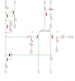
On the schematic:
Do a Tools > ERC, fix issues.
Check V+ on R3 and R12. There is a wire overlap and it may not be connected to V+. Drag V+ and check the wire rubber bands.
Fix positioning of component labels especially the transistors.
No output terminal.
It is a little unusual they way you have represented your rails.
On the PCB:
Do a tools > DRC, fix issues.
All traces should be mitred 45 degrees, you missed some.
A few missing traces at C1, R13 and R4.
What size are the resistors? They look a little big.
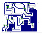
Ground planes are created by using the polygon command. Create a polygon (on the trace layer) matching the PCB border. Using the Name command, name the polygon the same as the ground net. Use the Ratsnest command to fill the polygon.
Use a vector font on the PCB. Options > User interface > Persistent in this drawing.
regards
Greg
A good start. Just a couple of comments.
On the schematic:
Do a Tools > ERC, fix issues.
Check V+ on R3 and R12. There is a wire overlap and it may not be connected to V+. Drag V+ and check the wire rubber bands.
Fix positioning of component labels especially the transistors.
No output terminal.
It is a little unusual they way you have represented your rails.
On the PCB:
Do a tools > DRC, fix issues.
All traces should be mitred 45 degrees, you missed some.
A few missing traces at C1, R13 and R4.
What size are the resistors? They look a little big.
Ground planes are created by using the polygon command. Create a polygon (on the trace layer) matching the PCB border. Using the Name command, name the polygon the same as the ground net. Use the Ratsnest command to fill the polygon.
Use a vector font on the PCB. Options > User interface > Persistent in this drawing.
regards
Greg
Last edited:
Thanks for the info!
I didn't know the method for filling a polygon. Thanks. My ground plane is a mix of squares and lines.
As for the schematic, it is a quick partial transcription of a schematic I did in LTSpice, and not intended to be "functional" per se. That said, I did miss what you noticed.
The rails were an attempt at learning the "name" command. O the ltspice schematic, they are done the usual way.
The resistors are supposed to be 2 watt metal film resistors that I have. The real part is probably 1/2" long. I probably will try to match the part better in a real PCB.
I noticed the missing traces after I uploaded the image.
What I am most curious about is what you think about my component placement and routing decisions, particularly the rails.
@ilmzn:
Care to expound on the use of ground planes? I had wanted it to be more "pervasive" throughout the board, but it ended up just on one end. My understanding is a ground plane needs to create as little impedance between the components and the final start point. In that regard I thought I did ok, but maybe I didn't do this right.
The other thing I understand ground planes are for is to provide some emf shielding. I am certain that having my plane only in one quadrant of the board doesn't accomplish this at all. Any thoughts on how to get the plane to "reach" more of the board? I kept getting pinned in corners.
About the holes. Why exactly do I need to etch them? Is there a reason I can't just drill through the copper in the middle of the pads? There must be a reason, because everyone does it. I can't just leave a minimal hole just to aim the drill with?
I agree and have said the same in previous Threads...........6) Do NOT use ground planes if you don't know how they work, what they are for and how they are used!!!! Using a ground plane is FAR more than just using a polygon fill even if it does look good - you can actually get worse results if it's not done properly, and from your example it's obvious you don't know how to do this. Use just plain tracks, to get a properly connected board first, then this can be optimized..........
I am beginning to understand Ground Planes as I am now just past half way through H.Ott, but I would still not try to design a ground plane into any of my implementations.
As a drill guide that is centred on the correct location is a good enough reason for me............ I can't just leave a minimal hole just to aim the drill with?
Do you know how to sharpen a drill?
Practice on a big one one (10mm) until you get the grinding angles and rotations right before you attempt a 3mm drill. Then get that right before you attempt a 1mm drill.
I have just about managed a sharpening of a 0.7mm drill, but my magnification cannot show how bad my angles are.
- Status
- Not open for further replies.
- Home
- Amplifiers
- Solid State
- Critique my first PCB routing attempt