Hello,
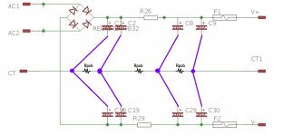
I am planning to make a CRC PSU for Class A (Jean Hiraga), which can also be used for class AB.
The PCB layout is made in 2 styles.
I have made 2 layouts and wish to know which one is the recommended one.
Attached are the schematic, Layout A, and Layout B.
Thanks and regards,
Sumesh


I am planning to make a CRC PSU for Class A (Jean Hiraga), which can also be used for class AB.
The PCB layout is made in 2 styles.
I have made 2 layouts and wish to know which one is the recommended one.
Attached are the schematic, Layout A, and Layout B.
Thanks and regards,
Sumesh

Both layouts are worse on force current routing. It will work but filter and storage capacitors are not routed correctly.
It needs to go from pad to pad to force current flow throught capacitor. Ground and rail connections needs wider track as there will be flowing 5A max current. At schematic there is missing rc filter at output....add kelvin sensing at output connections and many ground connectors...routing pcb for psu is not as easy task...waiting for new revisited layout....
It needs to go from pad to pad to force current flow throught capacitor. Ground and rail connections needs wider track as there will be flowing 5A max current. At schematic there is missing rc filter at output....add kelvin sensing at output connections and many ground connectors...routing pcb for psu is not as easy task...waiting for new revisited layout....
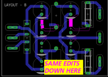
If you're hoping to implement Bob Cordell's excellent suggestion "Star On Star Grounding" you'll want to route the electrolytic caps and the common (0V) signal as shown in the attached figure. It appears to me that implementing this would require fewer edits to Layout B than to Layout A. Both require edits; but I think A requires more edits.
_
_
Attachments
You can create a ground plane with the polygon option either on layer 1 or 16 and name it GND, use properties to set the clearance required.
Thank you.You can create a ground plane with the polygon option either on layer 1 or 16 and name it GND, use properties to set the clearance required.
A polygon connected to CT...?
Thanks.Are you limiting yourself to a single-sided PCB?
Are you limiting this layout to only the 4-pin, in-line single diode bridge?
I am ready to use any package for diode and a 2 layer PCB for improvements.
Kindly provide your suggestions.
HI,If you're hoping to implement Bob Cordell's excellent suggestion "Star On Star Grounding" you'll want to route the electrolytic caps and the common (0V) signal as shown in the attached figure. It appears to me that implementing this would require fewer edits to Layout B than to Layout A. Both require edits; but I think A requires more edits.
_
I have changed the tracks to get 2-star points. Please find the image below:
Expecting your feedback.
Hi,Both layouts are worse on force current routing. It will work but filter and storage capacitors are not routed correctly.
It needs to go from pad to pad to force current flow throught capacitor. Ground and rail connections needs wider track as there will be flowing 5A max current. At schematic there is missing rc filter at output....add kelvin sensing at output connections and many ground connectors...routing pcb for psu is not as easy task...waiting for new revisited layout....
Thanks for the input.
Can you please elaborate on how to force current routing? a diagram would be of great help.
I shall widen the ground track once the layout is finalized.
Thanks
I am ready to use 2 sided PCB and TO220 diodes. I am confused in the routing of tracks connecting the capacitors.Are you limiting yourself to a single-sided PCB?
Are you limiting this layout to only the 4-pin, in-line single diode bridge?
The ingress current from the bridge rectifier is very dirty. It should reach the capacitor via a segregated path with respect to the egress current path, which must have less ripple (and RF noise), if the capacitor is given the opportunity to work at its best. So, the below design is not good... the tracks are mixed together:

Study the PCB layout of Japanese amplifiers - Marantz for example.
With power amps, it is easier to achieve correct power supply capacitor topology and grounding without the PCB.... but the PCB looks better...
Edit: two capacitors can be connected together via a thick/wide PCB track, and then assumed to be a single one (single capacitor)... but the above rule should be respected... hence, it is easier to get the thing right without the PCB... especially if the capacitors with the screw terminals are chosen; you get everything right by default 🙂
Last edited:
The ingress current from the bridge rectifier ... should reach the capacitor via a segregated path with respect to the egress ...
Pretty easy to achieve by a few edits in pink. Sorry that rectangles are filled in while non-rectangles are not. Novice user of mspaint.
_
Attachments
Thanks for the inputs.
I shall edit the layout and post it here soon.
Thanks and regards,
Sumesh
I shall edit the layout and post it here soon.
Thanks and regards,
Sumesh
- Home
- Amplifiers
- Power Supplies
- CRC PSU PCB for Class A/AB amps