It's old wisdom, the sound and specs of a power amplifier are mostly determined by its output stage. Hence, well designed output stage is the foundation of a good power amp. Among variety of topologies aiming for maximum linearity, I was intrigued by theoretic possibility to exploit MOSFET's quadratic transfer characteristic in an A-class push-pull setup that exhibits linear overall transfer function. Moreover, such setup could have linear equivalent output resistance (which is at least equally important for the overall tonal character).
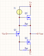
There are various implementations taking advantage of this feature to certain degree. The PLH Amplifier PassDiy is one of them and I took some time contemplating possible improvements. The core of PLH design consist of two output MOSFETs (Q2 & Q3) and a transistor Q1 (originally another MOSFET) in a double role of voltage amplifier and phase splitter. Feedback loop R1 & R2 is crucial for normal operation.
There are various implementations taking advantage of this feature to certain degree. The PLH Amplifier PassDiy is one of them and I took some time contemplating possible improvements. The core of PLH design consist of two output MOSFETs (Q2 & Q3) and a transistor Q1 (originally another MOSFET) in a double role of voltage amplifier and phase splitter. Feedback loop R1 & R2 is crucial for normal operation.
Attachments

I realized, a slight modification can transform it in an output stage with promising features. Although I cannot recollect seeing this topology elsewhere I would be surprised if this was not tried before. I will tentatively call it chip PLH follower or CPLHF.
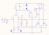
As depicted, Q1 is replaced with a P-type device. The change brings some new features:
- Obviously it’s non-inverting amp now
- It’s a voltage follower with gain slightly less than 1
- No need for overall feedback (R1 & R2 are gone)
- Input impedance is very high
- Q3 is now driven from low impedance while Q2 sees still relatively low Rgs
- When stimulus comes from input side, Q1 acts as source follower driving the gate of Q3 and simultaneously a phase splitter providing opposite change of Vgs to Q2.
- When stimulus comes from the output, Q1 acts as a folded cascode and mirrors the change of Vgs of Q3 to Vgs of Q2 (with opposite sign of course).
- Voltage amplification of Q1 is <1, so Miller Effect on its Cds is negligible.
Attachments
Obviously, the next logical step is to build an amp based on CPLHF for the proof of concept. A headphone amp is suitable project for this purpose. I decided first to build the output stage only and evaluate its real life performance. Decision about the rest would come later.
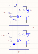
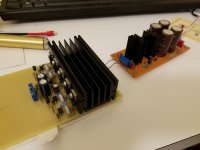
So this is how a real world implementation of CPLHF ended up (one channel).
The real world MOSFETs need gate stoppers and overvoltage protection for safe operation (D1, D2, R3 & R4). Further safety comes from current limiting implemented by R5 – R8, U1 & U2. This should prevent output current going beyond 350 – 400mA. (Also R5 and R6 are convenient for measuring the bias current).
Attachments
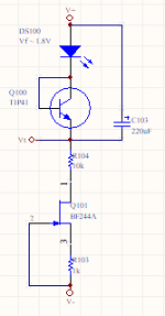
Output MOSFET’s have no source resistor in order to maintain quadratic character of the transfer function. The bias current is stabilized by thermal compensation. Current source I1 is implemented by Q4, R9 R10. I1 is proportional to Vt voltage reference which is temperature dependent. Bias current is adjusted by turning R10.
Vt voltage reference is shared by both channels. There is a single circuit generating it. Power transistors of both channels (4 x IRF510) and temperature sensing Q100 (1 x TIP41) are mounted on a single heatsink, about 2cm apart from each other.
Vt voltage reference is shared by both channels. There is a single circuit generating it. Power transistors of both channels (4 x IRF510) and temperature sensing Q100 (1 x TIP41) are mounted on a single heatsink, about 2cm apart from each other.
Attachments

Testing went fine. After several iterations of bias adjustment, the bias current remained relatively stable around 100mA, drifting < +/- 5%. When fed with signal form a smartphone, reproduction was clear and undistorted.
In standalone use, output DC offset drifts over wide range so the use of output capacitor is commended. The lack of suitable capacitors at hand discouraged me from going through extensive listening evaluation and I proceeded impatiently with building appropriate front end. (If standalone operation is needed, DC servo can be used to eliminate the output cap, but the input cap would still be needed.)
In standalone use, output DC offset drifts over wide range so the use of output capacitor is commended. The lack of suitable capacitors at hand discouraged me from going through extensive listening evaluation and I proceeded impatiently with building appropriate front end. (If standalone operation is needed, DC servo can be used to eliminate the output cap, but the input cap would still be needed.)
Attachments
Using an opamp at front and closing overall feedback loop around CPLHF and the opamp is the simplest and fastest way to build complete amp with low distortion, low output impedance, low DC offset and drift, etc. However, having custom tailored discrete front end would better reveal potentials of the CPLHF.
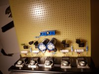
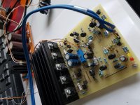
Instead of more modern CFB topologies I picked an old-timer topology typical for Hitachi amplifiers from mid ‘70s for good sound, familiarity, low DC offset (important for HPA) and mild thumps on power on/off (no need for output relay). In this “cover version” I replaced BJTs in some positions with JFETs and MOSFETs but the price was the need for tight matching from handful of devices in order to achieve reasonably low DC offset (BJT-only front end would be much easier to build). I did also some other enhancements, yet avoiding excessive complexity.
Instead of more modern CFB topologies I picked an old-timer topology typical for Hitachi amplifiers from mid ‘70s for good sound, familiarity, low DC offset (important for HPA) and mild thumps on power on/off (no need for output relay). In this “cover version” I replaced BJTs in some positions with JFETs and MOSFETs but the price was the need for tight matching from handful of devices in order to achieve reasonably low DC offset (BJT-only front end would be much easier to build). I did also some other enhancements, yet avoiding excessive complexity.
Attachments
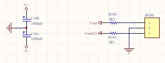
Note that I bypassed C13 since DC offset ended up reasonably low 11mV. So this prototype has no caps in the signal path. Attached are the parts shared to both channels. (I retrofited simple circuit that kills the bias current when supply voltage goes on/off but will submit it later).
Attachments
Nice circuit. And impressively clean construction (makes my prototype stuff look terrible in comparison!). Any measured data on this?
Attachments

@bwaslo unfortunately I can't present standard spec measurements. I don't have proper equipmet for that, maybe I'll figure out how to make usefull distortion spectrum measurement with my PC.
However, some specs can be reasonably estimated from calculaton and watching waveforms on the scope.
However, some specs can be reasonably estimated from calculaton and watching waveforms on the scope.
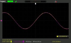
Response to sine and square excitation with (I think) 20R load (ch1 input ch2 output)
Intrinsically, the bandwidth is up to few hundreds kHz width but the main limiting factor is the input RF filter. With 25k pot on input it is about 200kHz depending on pot position.
Intrinsically, the bandwidth is up to few hundreds kHz width but the main limiting factor is the input RF filter. With 25k pot on input it is about 200kHz depending on pot position.
Attachments

Last edited:
- Status
- Not open for further replies.
- Home
- Amplifiers
- Solid State
- CPLHF output stage