Its usually a good idea.
I always connect my copper pours to zero volts so it acts like a screen.
Connecting to zero volts also reduces the impedance of the zero volt line which is good.
However you still need to use star grounding to reduce hum especially if there is a power supply on board.
I always connect my copper pours to zero volts so it acts like a screen.
Connecting to zero volts also reduces the impedance of the zero volt line which is good.
However you still need to use star grounding to reduce hum especially if there is a power supply on board.
I would rather just point-to-point something that simple - possibly on clearance hole gnd plane perfboard
performance can be better, power wires tightly twisted, 1 or 2 cuts with X-Acto peeling up copper to isolate a strip of plane for a bus...
unless you need more copies of the circuit it often isn't worth dealing with the chemicals, safe disposal, holes in you clothing... for such a simple PCB
after 30 years of EE employment I can assure you various hand prototyping techniques are in fact "professional" - many test/calibration circuits on factory floors, production benches are made "by hand" - no PCB etching ever involved
Linear Technology showed advanced "dead bug" protoyping - used to demonstrate STOA (ca. 1990 - but more than adequate for "audio") performance of their chips http://cds.linear.com/docs/en/application-note/an47fa.pdf
you will get other opinions from "PCB Hobbyists" - who may have 100's of hours experience, dedicated setups - but I like to keep the alternatives open for those who may mistakeningly think that making a PCB is the only path to making a working, usable electronic circuit
Last edited:
after 30 years of EE employment I can assure you various hand prototyping techniques are in fact "professional" - many test/calibration circuits on factory floors, production benches are made "by hand" - no PCB etching ever involved
We occasionally used wire wrapping for one off systems.
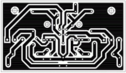
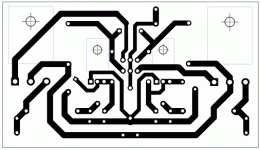
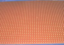
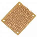
jcx, by clearance hole ground plane perfboard, do you mean attachment one or attachment two? I've prototyped lots of circuits on radio shack type perfboard as in the second attachment but I'm not sure if your referring to something else.
Attachments
We occasionally used wire wrapping for one off systems.
I used wire wrap quite a lot back in the 80s, but mainly for lower and medium speed digital. The socalled 'modified wrap' was developed for the Apollo program, I think...
works very good, but don't let the birds in....'cause it looks like...... 😀
I had a couple of PCBs made last year with the copper pour, the circuit was only a high speed buffer for data but the extra copper made the board oscillate horribly.
Only use copper pours if you can tie the copper to your 0V *(or ground).
Katieanddad, I would be interested in why you had problems, we copper pour on high speed boards and don't have any problems what so ever (Up in the low GHz digital designs). Did you have a contiguous ground plane that you can stich the copper pours down to using vias.
Copper pours are also used on sensitive analogue designs, again these tend to be multi-layer designs with at least on solid contiguous ground plane.
You do have to use stiching vias, and avoid long slivers of poured copper without a via at each end (a sliver will act like a dipole and can pick up noise).
There was some discussion of "ground plane" layers in another thread.
Apparently, some times it is not a good thing, other times it is.
It adds some capacitance to ground inevitably.
_-_-
Apparently, some times it is not a good thing, other times it is.
It adds some capacitance to ground inevitably.
_-_-
For digital it is mandatory with todays high speed and more importantly fast rise times, in fact there are very few situations or boards that I work on that do not have ground planes. Some RF boards you have to be careful and clear the ground away from certain tracks on board antennas, and on PCIe interface you have to clear the ground from under the DC coupling caps, but other than that all boards I see (apart from the real bargain basement boards) have a multilayer construction with a minimum of one contiguous ground plane and more often than not more.
I would be interested in reading the thread.
I would be interested in reading the thread.
Sorry, no clue which thread that bit spewed forth!
It did come from a knowledgeable poster, or I would have disregarded the comment. Doesn't help here much, but that's all I have.
It did come from a knowledgeable poster, or I would have disregarded the comment. Doesn't help here much, but that's all I have.
For audio, I don't think the added capacitance could be a problem. It could be a benefit actually.
- Status
- Not open for further replies.
- Home
- Design & Build
- Construction Tips
- Copper Pours