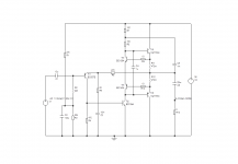
As there seemed to be some interest in a complementary version of John Linsley Hood's 10W amplifier I've started this thread to see what pans out.
I've not built this, but it seems to behave in simulations and is stable in a Tian probe with 60 degree phase margin and 40dB gain margin similar to the original.
It's a bit watty in the driver stage, and needs 2W 100 ohm load resistors. The driver transistor also needs a good heatsink - or mounting on the output transistor heatsink as it dissipates 2W. It could probably manage 40V (up to 16W output 8 ohm load) as its second breakdown (as originally published by Mullard) is getting close. The standing current is estimated at 1.5A.
Distortion simulated at under 0.1% at 20kHz and 10W.
Attachments
No, I don't use LTSpice!
mjona posted one in the JLH10 thread (#6459) which could be used as a start.
mjona posted one in the JLH10 thread (#6459) which could be used as a start.
Last edited:
OK, but why would you do that?John
I think that one of advantage of complementary A-class OPS is that front end can be also reversed ,so Q1 can be N-type and Q2 P-type .
OK, but why would you do that?
well , if that option exist than why not to try that version also and to compare with first version ? 🙂
Allison bias; the circuit looks clean; and you can also introduce a "tweak" point: if you connect a pot/rheostat between T3/T4 bases, you can then set-up a standing current with it... perhaps with slight readjustment of the neighbouring components in the sim?
Basically yes , pot can be connected between Q3/Q4 bases , but also couple of series connected diodes + pot , where diodes will be attached on the main heatsink to regulate OPS- Iq ,
or even some standard one transistor Vbe multiplier can be also connected there ,
but John solution with two transistors for automatic bias adjustment is one very very good solution too.
or even some standard one transistor Vbe multiplier can be also connected there ,
but John solution with two transistors for automatic bias adjustment is one very very good solution too.
Member
Joined 2009
Paid Member
JLH uses v few parts and I wonder if tr3 and tr4 could be removed if wanting the simplest starting point?
The Allison bias circuit is ideal for this I think. The bias transistors do not have to be mounted on the main heatsink as the feedback will set the output stage current. The collector impedance is high, and won't care too much about the output device Vbe.
A simpler approach would be to use a resistor but that would change the current drop across it during signal swings and probably increase distortion (not tested). At the least I would use a couple of diodes like 1N4002 which could be mounted on the heatsink, one next to each transistor, to compensate for Vbe changes. That would allow a smaller resistor to be used with less potential effect on distortion. On balance a couple of transistors (with base stopper resistors) is only one component more than two diodes and a resistor!
A simpler approach would be to use a resistor but that would change the current drop across it during signal swings and probably increase distortion (not tested). At the least I would use a couple of diodes like 1N4002 which could be mounted on the heatsink, one next to each transistor, to compensate for Vbe changes. That would allow a smaller resistor to be used with less potential effect on distortion. On balance a couple of transistors (with base stopper resistors) is only one component more than two diodes and a resistor!
Almost automatic in operation
I used a 30 watt into 8 ohms class A design driving a pair of B+W DM6
Sounded great
Even built an oil cooled version with TO3 devices lids cut off so that the oil could get to the chips sounded good but after a few hours all i could smell was hot oil
Trev
I used a 30 watt into 8 ohms class A design driving a pair of B+W DM6
Sounded great
Even built an oil cooled version with TO3 devices lids cut off so that the oil could get to the chips sounded good but after a few hours all i could smell was hot oil
Trev
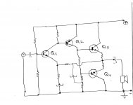
In my simulations for practical purposes C4 makes no difference to the THD all it does is bypass TR3 and TR4 whose linearity we should look at as it would have to be very good.
This is a factor which is enhanced by R9 and R10 which swamp the bases of TR3 and TR4 and so the small non-linear resistor in the emitter is less important in the forward conduction path. The voltage drop across R9 and R10 will be far greater than that across the diode emitter resistance.
One can increase these values to increase the output stage standing current in small increment and enhance the base swamping effect further. I looked at increasing the values to 22R and 100R.
While a diode string could be used, two 1N4148 diodes is not going to generate enough voltage drop so a resistor in series would be necessary. The voltage drop required is in excess of three 1N4148's.
If you go this way one would use two off in the hope the compensating resistor value falls in the standard range for adjustment purposes.
Not evaluated your observations, yet, mjona, but I suggested 1N4002 diodes because the current in the driver stage is approaching 100mA - the 1N4148 is only rated to 75mA.
Driver current could probably be reduced if high gain OP transistors are used like MJL3821/1302. Whether stable is another issue to check. THe main reason for including C4 was for the purposes of using these devices. Keeping the bases tightly coupled seems to give better stability in other simulations.
Driver current could probably be reduced if high gain OP transistors are used like MJL3821/1302. Whether stable is another issue to check. THe main reason for including C4 was for the purposes of using these devices. Keeping the bases tightly coupled seems to give better stability in other simulations.
John
I think that one of advantage of complementary A-class OPS is that front end can be also reversed ,so Q1 can be N-type and Q2 P-type .
Le Ultra-low Distortion Class-A Amplifier de L. Nelson-Jones : Wireless World (03/1970)
nj10w.pdf
6.9 Schemas - francis.audio
Nothing can be invented. Everything that you come up with, was either invented before you, or it really happens.
Arkady and Boris Strugatsky
Last edited:
Le Ultra-low Distortion Class-A Amplifier de L. Nelson-Jones : Wireless World (03/1970)
nj10w.pdf
6.9 Schemas - francis.audio
Nothing can be invented. Everything that you come up with, was either invented before you, or it really happens.
Arkady and Boris Strugatsky
-That Nelson-Jones A-class amp have nothing in common with this extra simple -Complementary JLH A-class amp .
-And show me where did I have claimed that I have invented this extra simple circuit ?
-That Nelson-Jones A-class amp have nothing in common with this extra simple -Complementary JLH A-class amp .
-And show me where did I have claimed that I have invented this extra simple circuit ?
You did not say this)
But this is a simple Lin scheme)
JLH has a similar scheme to Le JLH 1970 de J. L. Linsley Hood: Wireless World (07/1970)
http://www.tcaas.btinternet.co.uk/jlhab2.htm
Not evaluated your observations, yet, mjona, but I suggested 1N4002 diodes because the current in the driver stage is approaching 100mA - the 1N4148 is only rated to 75mA.
Driver current could probably be reduced if high gain OP transistors are used like MJL3821/1302. Whether stable is another issue to check. THe main reason for including C4 was for the purposes of using these devices. Keeping the bases tightly coupled seems to give better stability in other simulations.
I think that use of very high speed and very high Hfe complementary power pair is very good choice ,
in that manner I suggest use of even faster 2SC2565/2SA1095 power pair ,but with highest Hfe 120-240 (Y) class .
No Free Lunch
With respect to your Allison version using those transistors, for stability a combination is indicated for a capacitor between the collector of TR2 and the emitter of TR3 and an 8R2+100nF zobel network at the output.
With MJL21193/MJL21194 for the same reasons, as with the original JLH these would set the dominant pole and the compensation capacitor could be omitted.
My advice is to stay away from the diode bias scheme altogether. While that may appear to reduce the component count the peak current flow through the diodes does not exceed much more than 50 m.a. in my tests.
In comparison with an active bias scheme like the Allison one this is a handicap which impacts on stability and power output raising the question about adding extra components. This presents as simplification in one area making for complexity in other areas where that is undesirable.
Not evaluated your observations, yet, mjona, but I suggested 1N4002 diodes because the current in the driver stage is approaching 100mA - the 1N4148 is only rated to 75mA.
Driver current could probably be reduced if high gain OP transistors are used like MJL3821/1302. Whether stable is another issue to check. THe main reason for including C4 was for the purposes of using these devices. Keeping the bases tightly coupled seems to give better stability in other simulations.
With respect to your Allison version using those transistors, for stability a combination is indicated for a capacitor between the collector of TR2 and the emitter of TR3 and an 8R2+100nF zobel network at the output.
With MJL21193/MJL21194 for the same reasons, as with the original JLH these would set the dominant pole and the compensation capacitor could be omitted.
My advice is to stay away from the diode bias scheme altogether. While that may appear to reduce the component count the peak current flow through the diodes does not exceed much more than 50 m.a. in my tests.
In comparison with an active bias scheme like the Allison one this is a handicap which impacts on stability and power output raising the question about adding extra components. This presents as simplification in one area making for complexity in other areas where that is undesirable.
- Home
- Amplifiers
- Solid State
- Complementary JLH10