In my SIT-3X Amplifier thread I asserted that the common-drain PFET subcircuit of the SIT-3X utilized Schade feedback. Amplifiers described in other threads, in particular some of Zen Mod's designs, have utilized similar common-drain "Schade" feedback circuit.
In this thread I claim that the common-drain Schade-like circuit does not have any feedback other than from the ground, or the input signal reference ground. Thus, the resistor divider performs input signal attenuation rather than feedback.
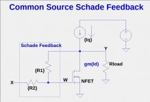
The first schematic shows a "classical" common-source Schade circuit where the resistor divider formed by R1 and R2 "mixes" the input signal with the output signal, which is inverted, forming a negative feedback circuit. It is easy to verify the negative feedback behavior by both simulation and circuit analysis.
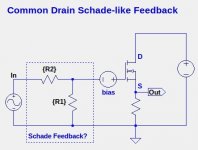
The second schematic shows a common-drain (aka. source-follower) circuit with the appearance of Schade Feedback. If you carefully examine the upper connection of resistor R1 it has the same AC signal level as ground (except for power supply ripple), as shown in the first schematic. Thus the AC signal at the gate of the FET is an attenuated version of the signal of the input IN. There is no feedback from the output.
In this thread I claim that the common-drain Schade-like circuit does not have any feedback other than from the ground, or the input signal reference ground. Thus, the resistor divider performs input signal attenuation rather than feedback.
The first schematic shows a "classical" common-source Schade circuit where the resistor divider formed by R1 and R2 "mixes" the input signal with the output signal, which is inverted, forming a negative feedback circuit. It is easy to verify the negative feedback behavior by both simulation and circuit analysis.
The second schematic shows a common-drain (aka. source-follower) circuit with the appearance of Schade Feedback. If you carefully examine the upper connection of resistor R1 it has the same AC signal level as ground (except for power supply ripple), as shown in the first schematic. Thus the AC signal at the gate of the FET is an attenuated version of the signal of the input IN. There is no feedback from the output.
Attachments


now, if instead Schade Feedback, that arrangement with increased gate resistor value and included D-G resistor, you call it Schade Effect, is there any difference in thinking?
see, situation is rather ..... not so simple
for instance - complementary pair of mosfets, connected as simple source follower OS - we all know what is it
if you introduce Schade Effect resistor pair to upper one (frankly, same happens if you bring it to lower one) , you're getting Poor Man's DEF stage, Schaded mosfet being replacement for depletion/SIT
catch is that it works, while output for that (Schaded) part is from source node
well, can't think further than that tonight, time to zzzz
Last edited:
In a common-drain, push-pull configuration the resistor divider is useful to reduce the effective gm (transconductance) of FET, making it possible to the balance the AC currents of the two FETs without needing source resistors.
In the SIT-3X common-drain 2SK182ES/IXYS-PFET case, it was necessary to reduce the gm of the PFET in order to prevent the "pull-pull" behavior of the circuit, without using source resistors. I will describe my observations about this in a later post. I think you will find it interesting.
In the SIT-3X common-drain 2SK182ES/IXYS-PFET case, it was necessary to reduce the gm of the PFET in order to prevent the "pull-pull" behavior of the circuit, without using source resistors. I will describe my observations about this in a later post. I think you will find it interesting.
While perhaps not what Schade was thinking, it remains a clever hack to adjust 2nd harmonic.

In the second and third circuit, I am not sure there is any feedback. As you have shown, it is a resistor from gate to ground, and nothing is changing at ground, which is why it is ground.
Alternatively, you could put a small value resistor between drain and ground and develop an AC voltage that would then be fed back.
Alternatively, you could put a small value resistor between drain and ground and develop an AC voltage that would then be fed back.
A resistor between drain and ground would just add a current across the power supply.In the second and third circuit, I am not sure there is any feedback. As you have shown, it is a resistor from gate to ground, and nothing is changing at ground, which is why it is ground.
Alternatively, you could put a small value resistor between drain and ground and develop an AC voltage that would then be fed back.