What should a DIY-Audio novice build first. The WWW has suggested the famous CMoy headphone amp as a good novice project but I think we should construct a few projects that are easier and more robust for the novice. The following is my effort to offer such a project which I hope the novice will find buildable or interesting.
(Newbie, newb, noob, noobie, n00b is a slang term for a novice)
Legacy Projects: CMoy is a portmanteau of Pow Chu Moy who created a minimilist headphone amplifier that people could build with parts from Radio Shack. The original was in a plastic box with an opamp and a battery. It had a high-low switch for volume control. The HeadWize site showed many variants especially the Altoid Tin version. Mr Moy has passed away and HeadWize is gone but someone created a memorial site without the lost forums. [Memorial]
Next, there is the comprehensive tutorial provided by Tangentsoft [Audiologica]. It suggests that the CMoy pocket amp is an excellent choice for your first DIY audio project. I agree except that the tin can enclosures and rail-splitter power supply are not required for a desktop unit.
Prerequisites: You need to do soldering, drilling, and multimeter measurements. You need to have keen interest in doing it.
Shopping: You need to satisfy the Bill of Materials (BOM). Most parts are from Mouser. There are a few items from Amazon.
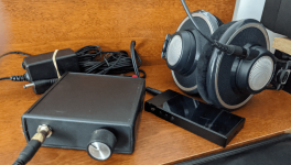
System: Here are two images showing the completed system recently tested. The front panel 1/4 jack connects AKG K702 headphones. The K702 demands more drive for it's 62 ohm impedance. It is not a problem for this single opamp JRC4556AD in single-supply mode. The power supply is Triad 15vdc. I did not test with 24vdc which is not required. The back panel has a DC jack and two single RCA jacks for input from the FiiO line output.


Enclosure: The enclosure is a Hammond Box with standoffs for 2 BusBoard Systems size1 PCBs. This box has removable front and rear panels for easy drilling. This project uses panel mount jacks and volume pots. Panel mounting requires a bigger box but does not require the precise panel measurements of an integrated PCB.
The selected Hammond Box has room for two size1 PCBs or 1 PCB which can be in 3 positions ... front, center, or back. With one PCB only, the box has more room for panel mounts. There are six standoffs in the base and 4 more in the cover.
PCBs: Busboard has 3 types of size1 (80x50mm) PCB. There is stripboard, proto board, and PadBoard. PadBoard is best since it is double-sided with plated-thru holes. Solder flows into the thru-hole such that a good connection can be made without solder blobs. And it is easy to desolder cleanly. Only the PadBoard has a square pad every 5th hole for easy placement of parts in 31x19 holes. I provide a layout plan to visualize the end result before starting installation.
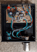
Top View: Here is the Amp with the top cover removed. It reveals a few flaws caused by all the standoffs. The PCB is in rear position to leave more room for the front panel wires. The PCB can be in the center positon if smaller wiring is installed. The volume pot needs to be installed closer to center so that it can be rotated to feed shorter wires along the side. The phone jack needs to be closer to center because the cover has standoffs for a size2 PCB. The cover can close but it rubs the phone jack a bit.
My build has flaws or bugs but the plan is updated to resolve them.
Schematic: This first build does not include an integrated power supply. Instead it is biased for single-supply operation so that a 15vdc wall adapter can be used. D1 protects against accidental reverse-voltage. D2 indicates when the unit is active. R2 and R3 provides 7.2vdc for opamp bias. C7 and C8 protects the headphones against DC voltages. There is a special power-on procedure to prevent noises from capacitor charging. Wait a few seconds before connecting headphones. The caps will charge through R10 and R11.
Mr Moy advised CMoy builders to use disposable headphones since they are not protected in the minimalist rail-splitter (virtual-ground?) design. TangentSoft has a whole page explaining virtual ground variations. Given all the explaining, there is no way to make it robust. And novice projects need to be robust.

PCB Plan: The PCB is modelled with VeroRoute (VR) as a 1-sided unit. The connections are routed automatically but constrained. For example, VR Tracks cannot cross each other but VR Wires can. IC1-1 connects to C7 and R9 via a purple VR Track, which is a bare wire on the PCB underside. IC1-2 connects to R9 via a pink VR Wire which crosses the IC1-1 VR Track (an insulated wire on the top side). There are no tracks on the PadBoard, connections are physical wires between the component pins.
Sometimes VR will take an awkward route as it recursively searches for a good path. In that case, I add labelled pads or VR wires to guide it to a preferred path. At other times, the autoroute is too complex making the plan hard to read. For example, IC1-5 needs to connect to C6-R5. There is no connection in the PCB model, just U5 labelled pads. The connection is completed by adding a top-side insulated wire U5 to U5. It's easier to use this hybrid approach.
There are gaps between components for ease of soldering without creating short circuits. The circle-X symbols are non functional. I use them to mark pads that should be reserved.

Stuffing: Components are added to the PCB in phases. Phase 1 includes soldering the resistors and other components in their planned location. They should be lightly soldered on the under-side such that resistor leads are straight and cut short less than 5mm. These short leads are posts for the connecting wires. The PCB supports are 5mm. So install all the components to complete phase 1.
Phase 2: The under wires are installed in phase 2 where the component pins are wired according to the plan. Since the DIP socket has short pins for installation on a fabricated PCB. the PadBoard requires a custom procedure for the DIP. Insert a bare wire top-side, switch to the under-side and bend the wire to form an "L". Next, retract the wire until the end is flat on the PCB and touching the DIP pin. Solder gently. If this seems strange, you can try making a hook around the pin instead.
Use a temporary wire twist to hold the DIP in place for soldering.


Phase 3: The top-side insulated wires are installed in phase 3. These
are not shown in the plan. Here is a list.
U3: F5 ~ D14
U5: L4 ~ B14
U8: M8 ~ J21
!U4: J9 ~ R17
U4: C8 ~ H23
H1: H13 ~ C21
H2: I17 ~ C23


The BOM is attached. It is in Open Data Format.
(Newbie, newb, noob, noobie, n00b is a slang term for a novice)
Legacy Projects: CMoy is a portmanteau of Pow Chu Moy who created a minimilist headphone amplifier that people could build with parts from Radio Shack. The original was in a plastic box with an opamp and a battery. It had a high-low switch for volume control. The HeadWize site showed many variants especially the Altoid Tin version. Mr Moy has passed away and HeadWize is gone but someone created a memorial site without the lost forums. [Memorial]
Next, there is the comprehensive tutorial provided by Tangentsoft [Audiologica]. It suggests that the CMoy pocket amp is an excellent choice for your first DIY audio project. I agree except that the tin can enclosures and rail-splitter power supply are not required for a desktop unit.
Prerequisites: You need to do soldering, drilling, and multimeter measurements. You need to have keen interest in doing it.
Shopping: You need to satisfy the Bill of Materials (BOM). Most parts are from Mouser. There are a few items from Amazon.
System: Here are two images showing the completed system recently tested. The front panel 1/4 jack connects AKG K702 headphones. The K702 demands more drive for it's 62 ohm impedance. It is not a problem for this single opamp JRC4556AD in single-supply mode. The power supply is Triad 15vdc. I did not test with 24vdc which is not required. The back panel has a DC jack and two single RCA jacks for input from the FiiO line output.
Enclosure: The enclosure is a Hammond Box with standoffs for 2 BusBoard Systems size1 PCBs. This box has removable front and rear panels for easy drilling. This project uses panel mount jacks and volume pots. Panel mounting requires a bigger box but does not require the precise panel measurements of an integrated PCB.
The selected Hammond Box has room for two size1 PCBs or 1 PCB which can be in 3 positions ... front, center, or back. With one PCB only, the box has more room for panel mounts. There are six standoffs in the base and 4 more in the cover.
PCBs: Busboard has 3 types of size1 (80x50mm) PCB. There is stripboard, proto board, and PadBoard. PadBoard is best since it is double-sided with plated-thru holes. Solder flows into the thru-hole such that a good connection can be made without solder blobs. And it is easy to desolder cleanly. Only the PadBoard has a square pad every 5th hole for easy placement of parts in 31x19 holes. I provide a layout plan to visualize the end result before starting installation.
Top View: Here is the Amp with the top cover removed. It reveals a few flaws caused by all the standoffs. The PCB is in rear position to leave more room for the front panel wires. The PCB can be in the center positon if smaller wiring is installed. The volume pot needs to be installed closer to center so that it can be rotated to feed shorter wires along the side. The phone jack needs to be closer to center because the cover has standoffs for a size2 PCB. The cover can close but it rubs the phone jack a bit.
My build has flaws or bugs but the plan is updated to resolve them.
Schematic: This first build does not include an integrated power supply. Instead it is biased for single-supply operation so that a 15vdc wall adapter can be used. D1 protects against accidental reverse-voltage. D2 indicates when the unit is active. R2 and R3 provides 7.2vdc for opamp bias. C7 and C8 protects the headphones against DC voltages. There is a special power-on procedure to prevent noises from capacitor charging. Wait a few seconds before connecting headphones. The caps will charge through R10 and R11.
Mr Moy advised CMoy builders to use disposable headphones since they are not protected in the minimalist rail-splitter (virtual-ground?) design. TangentSoft has a whole page explaining virtual ground variations. Given all the explaining, there is no way to make it robust. And novice projects need to be robust.
PCB Plan: The PCB is modelled with VeroRoute (VR) as a 1-sided unit. The connections are routed automatically but constrained. For example, VR Tracks cannot cross each other but VR Wires can. IC1-1 connects to C7 and R9 via a purple VR Track, which is a bare wire on the PCB underside. IC1-2 connects to R9 via a pink VR Wire which crosses the IC1-1 VR Track (an insulated wire on the top side). There are no tracks on the PadBoard, connections are physical wires between the component pins.
Sometimes VR will take an awkward route as it recursively searches for a good path. In that case, I add labelled pads or VR wires to guide it to a preferred path. At other times, the autoroute is too complex making the plan hard to read. For example, IC1-5 needs to connect to C6-R5. There is no connection in the PCB model, just U5 labelled pads. The connection is completed by adding a top-side insulated wire U5 to U5. It's easier to use this hybrid approach.
There are gaps between components for ease of soldering without creating short circuits. The circle-X symbols are non functional. I use them to mark pads that should be reserved.
Stuffing: Components are added to the PCB in phases. Phase 1 includes soldering the resistors and other components in their planned location. They should be lightly soldered on the under-side such that resistor leads are straight and cut short less than 5mm. These short leads are posts for the connecting wires. The PCB supports are 5mm. So install all the components to complete phase 1.
Phase 2: The under wires are installed in phase 2 where the component pins are wired according to the plan. Since the DIP socket has short pins for installation on a fabricated PCB. the PadBoard requires a custom procedure for the DIP. Insert a bare wire top-side, switch to the under-side and bend the wire to form an "L". Next, retract the wire until the end is flat on the PCB and touching the DIP pin. Solder gently. If this seems strange, you can try making a hook around the pin instead.
Use a temporary wire twist to hold the DIP in place for soldering.
Phase 3: The top-side insulated wires are installed in phase 3. These
are not shown in the plan. Here is a list.
U3: F5 ~ D14
U5: L4 ~ B14
U8: M8 ~ J21
!U4: J9 ~ R17
U4: C8 ~ H23
H1: H13 ~ C21
H2: I17 ~ C23
The BOM is attached. It is in Open Data Format.
Attachments
Last edited: