I submit for discussion an amplifier that offers lower dissipation than class A, but could be made to sound "pretty close". I have simulated it in TINA-TI, using the fairly accurate model of the OPA134, and a model of the TIP142 that was found at element14. I tried to simulate with lateral MOSFET models, but there were some problems with the models I tried, namely that upon clipping to the rails, a spice error was generated regarding a diode specified in the .subcircuit file. Simulation below clipping seemed to work. Any help with good spice models for lateral MOSFETS that work with TINA would be most appreciated.
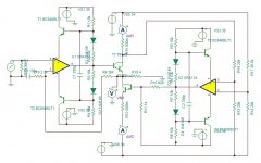
EDIT: 2 errors found in the first schematic, please refer to the one below.
EDIT: 2 errors found in the first schematic, please refer to the one below.
Attachments


Last edited:
Is there any explicit frequency compensation (besides what's inside the opamp packages)?
I worry that PSRR might be terrible, due to R11.
Also, PNP transistors T2 and T4 might be drawn upside-down. Probably you mean to connect their emitters to the opamps' negative power rail pins.
I worry that PSRR might be terrible, due to R11.
Also, PNP transistors T2 and T4 might be drawn upside-down. Probably you mean to connect their emitters to the opamps' negative power rail pins.
Drawing errors corrected
Was copy- and pasting blocks of that schematic around... thank you for locating those two errors.
First, the transistors that provide the negative supply to the opamps were accidentally upside- down.
Second, R11 was supposed to be connected to the (regulated and smoothed) rail for the opamps; It needs those rails to be higher than the output devices' rails, clearly, to allow for full swing operation controlled by the opamps. The higher voltage supplies are very low current and may be derived from voltage doublers from the main supply, then regulated. This should forgive the PSRR of the circuit.
Both corrections in new zip file.
The question of compensation is a good one. I tested with other opamp models and found stability issues, but the internal compensation of the OPA134 is robust, at least in simulation. I would add at lest, a zobel network, and possibly an inductor/ resistor in parallel for driving capacitive loads.
Attachments
Back to basics
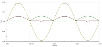
Here is a simulation of the core concept, stripped of servos to attain high voltage opamps. The slew rate was suffering too much when I added frequency compensation and a 10k square wave looked, well, not so square😛
This sim has frequency compensation and still makes decent square waves at 10khz. Next I will try OPA604 to get the rails higher (24v)😉
Attachments
My thoughts about the current control side:
The base of T5 will not be more than 2-3V away from VS6 power rail so the -Vcc to U2 will attempt to go to most of the way to VS4 (if possible) and +Vcc of U2 will be close to a couple of Volts above GND potential...I hope the common mode input range of U2 can swing that close to the +Vcc of U2 and the output can drive that close to the -Vcc of U2.
I would make a few changes to this cct.
1. skip VS3 and just use VS5, and skip VS4 and just use VS6
2. replace R10 with a 34V zener
In simulations you get a perfect rock solid power supply...not so easy in real life.
Have fun.
🙂
Just another comment.
The SOA (or SAO) of TIP142 is 40V or 45V (depends on who's datasheet you are viewing) at 2A.
You might want to consider multiple output devices for an actual build.
🙂
The SOA (or SAO) of TIP142 is 40V or 45V (depends on who's datasheet you are viewing) at 2A.
You might want to consider multiple output devices for an actual build.
🙂
It seems to me that you've got two amplifying stages in cascade: opamp U2, and common emitter amplifier T5. When the current in T5 is 1 ampere, its gm is 38.4 siemens, and so the gain contributed by T5 is (gm x rL) = (38.4 x 0.5) = 19.2X (across R15). T5 probably also contributes at least one pole to the system, meaning that the phase margin of the cascade is likely to be quite small.
I'd suggest that you break the loop (maybe at the R16-R15 junction?) and use AC analysis to make a Bode plot of the right hand feedback system. Put an AC source at the loop break, and remove any AC sources from the left half-circuit by setting their amplitude to zero.
I'd suggest that you break the loop (maybe at the R16-R15 junction?) and use AC analysis to make a Bode plot of the right hand feedback system. Put an AC source at the loop break, and remove any AC sources from the left half-circuit by setting their amplitude to zero.
24v rails with OPA604
I have been working at getting the compensation right, here is my best result so far... I have very little ringing and overshoot. Thank you for your suggestions, although I have not yet simulated them... If you have simulated anything successfully, please upload it if you find the time.
I have been working at getting the compensation right, here is my best result so far... I have very little ringing and overshoot. Thank you for your suggestions, although I have not yet simulated them... If you have simulated anything successfully, please upload it if you find the time.
Attachments

Some integrated amplifiers use a similar OP stage control. The first that comes to mind is the LT1010: www.linear.com/docs/1683
- Status
- Not open for further replies.
- Home
- Amplifiers
- Solid State
- "classless" amplifier simulation