So here it is: the COSDB (seems that abbreviations are hot in classD 🙂).
I've been looking at this forum for the past 10 years, and never before has so many classD-designs been available for us amateurs. But a lot of these designs apparently don't care about EMC, EMI and switch mode-circuits.
Chokoholic's thread here: http://www.diyaudio.com/forums/class-d/224052-systemd_2kw-any-interest-open-design.html looks like the most thought-through and ambitious project so far. I have no doubt that Chokoholic have forgotten more about classD than I'll ever know, but I still dare to present an alternative to his fantastic effort.
I'm thinking that "we" need a platform to experiment with classD. The platform I envision shall strive to meet these points:
I've done preliminary schematic and PCB-suggestion. I'm not sure that I'll find the time to actually build the amp, but the design-process is fun as well.
I'm hoping that all the knowledgeable members here will chime in and perhaps someone will make a few PCB's to verify the function.
We can never design a PCB that will fit every need or cater for every wish, - that's simply not possible with classD because space around the critical components are so limited.
The component-values on the presented schematic is not final. Some of them are probably way off. At this stage we are focusing on the connections in the schematic as these will dictate PCB-design.
PCB will follow if there is any interest.
Regards
I've been looking at this forum for the past 10 years, and never before has so many classD-designs been available for us amateurs. But a lot of these designs apparently don't care about EMC, EMI and switch mode-circuits.
Chokoholic's thread here: http://www.diyaudio.com/forums/class-d/224052-systemd_2kw-any-interest-open-design.html looks like the most thought-through and ambitious project so far. I have no doubt that Chokoholic have forgotten more about classD than I'll ever know, but I still dare to present an alternative to his fantastic effort.
I'm thinking that "we" need a platform to experiment with classD. The platform I envision shall strive to meet these points:
- TO220 mosfets on underside of PCB
- Only tracks on bottom of PCB. Top reserved for GND plane(s)
- Lots of SMD. 0805 minimum
- Best possible layout with regards to EMC, but still homemade
- Regulated supply for mosfet-driver and modulator
- Daughter-PCB's for: modulator, protection and Mosfet-driver
- Usable up to +/-65V, 10A minimum
- Usable as "real amplifier" but focus on development and learning
I've done preliminary schematic and PCB-suggestion. I'm not sure that I'll find the time to actually build the amp, but the design-process is fun as well.
I'm hoping that all the knowledgeable members here will chime in and perhaps someone will make a few PCB's to verify the function.
We can never design a PCB that will fit every need or cater for every wish, - that's simply not possible with classD because space around the critical components are so limited.
The component-values on the presented schematic is not final. Some of them are probably way off. At this stage we are focusing on the connections in the schematic as these will dictate PCB-design.
An externally hosted image should be here but it was not working when we last tested it.
PCB will follow if there is any interest.
Regards
Last edited:
A quick look at the PCB-suggestion. All red tracks are on the bottom, Green (looks yellow, sorry) is jumpers on bottom side.
White is (leaded)components on topside, yellow is (SMD)components on bottom.
Biggest compromise is the placement of the (big) output coil. The torroid is close to the Mosfets and therefore the switching node is as small as possible. This means that the PSU-caps are pushed away from the mosfets, but tracks are wide and loop-area are minimized. With a solid plane on the toplayer critical loops will be smaller.
On the proposed layout it is possible to place a shield between torroid and control-circuitry. All switchning-tracks and critical components are on bottoms-side and a solid layer on the top-side will confine the noisy parts between toplayer and heatsink.
Do-able, worthwhile or rubbish. Tell me.
Some of the notes used for inspiration:
AN-1135
AN-978
http://www.diyaudio.com/forums/class-d/111566-cool-small-2x150w-class-d-full-range-car-amplifier.html
Regards
White is (leaded)components on topside, yellow is (SMD)components on bottom.
An externally hosted image should be here but it was not working when we last tested it.
Biggest compromise is the placement of the (big) output coil. The torroid is close to the Mosfets and therefore the switching node is as small as possible. This means that the PSU-caps are pushed away from the mosfets, but tracks are wide and loop-area are minimized. With a solid plane on the toplayer critical loops will be smaller.
On the proposed layout it is possible to place a shield between torroid and control-circuitry. All switchning-tracks and critical components are on bottoms-side and a solid layer on the top-side will confine the noisy parts between toplayer and heatsink.
Do-able, worthwhile or rubbish. Tell me.
Some of the notes used for inspiration:
AN-1135
AN-978
http://www.diyaudio.com/forums/class-d/111566-cool-small-2x150w-class-d-full-range-car-amplifier.html
Regards
Attachments

Last edited:
This is looking like the birth of a nice experimental board. 😎
The footprint of L1 seems to overlap with the pins of M1 and M2. How is this intended in detail?
IRF530 has poor body diodes. Very high Qrr.
Hm, if you really want to use IRF530, you should use shottkys for freewheeling which ensure lower drop than the body diodes at any current. With normal diodes you will not prevent the body diodes from being flooded at higher load situations.
The entire Qrr topic in the half bridges is an interesting area, especially at high loads. IRF530 is for sure a scientifically interesting choice and examining its short comings and possible work arounds as well (gate drive timing and/or shottkys).
If you want the half bridge simple and trouble free - better use MosFets like IRF540Z, with phantastic body diodes and you won't need external freewheeling diodes.
Thanks for the input.
It might not be clear from the proposed layout, but there are no tracks on the topside below the toroid. The mosfets could be mounted SMD-style without drilled holes at all. - that way of mounting makes replacing the mosfets a lot simpler and the main switching nodes can be completely covered with a solid plane on top layer.
The 530 is just a quick pick from the component library. I'm guessing that IRF530 will only be used for this project if its the only part folks can get. - or if you happen to have a big pile in the stash. I've looked at the mosfet-selection From Farnell and it seems that we can get nice mosfets for 5$ and Ok ones for half.
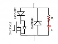
The diodes from D to S are meant to be fast ones. The symbol is just me being lazy and using the same for all diodes. I should update that. I have a pile of MUR340 rated at 400V / 3A for testing.
My biggest doubt so far is whether I should move the main capacitors closer right up to the mosfets on expense of longer connection to the toroid. Shorter current-path or bigger switching node? I like the current layout, but at the same time it looks like a linear amp layout which is rarely good...
With regards to GND-planes: any experience on the difference between solid gnd-planes and planes divided into:input-gnd, output-gnd and Vss as suggested in the previous mentioned ap-notes?
Keep the inputs comming
Kind regards
It might not be clear from the proposed layout, but there are no tracks on the topside below the toroid. The mosfets could be mounted SMD-style without drilled holes at all. - that way of mounting makes replacing the mosfets a lot simpler and the main switching nodes can be completely covered with a solid plane on top layer.
The 530 is just a quick pick from the component library. I'm guessing that IRF530 will only be used for this project if its the only part folks can get. - or if you happen to have a big pile in the stash. I've looked at the mosfet-selection From Farnell and it seems that we can get nice mosfets for 5$ and Ok ones for half.
The diodes from D to S are meant to be fast ones. The symbol is just me being lazy and using the same for all diodes. I should update that. I have a pile of MUR340 rated at 400V / 3A for testing.
My biggest doubt so far is whether I should move the main capacitors closer right up to the mosfets on expense of longer connection to the toroid. Shorter current-path or bigger switching node? I like the current layout, but at the same time it looks like a linear amp layout which is rarely good...
With regards to GND-planes: any experience on the difference between solid gnd-planes and planes divided into:input-gnd, output-gnd and Vss as suggested in the previous mentioned ap-notes?
Keep the inputs comming
Kind regards
Last edited:
...still not getting the MosFet-choke-overlap.
More detailed what I am wondering about:
MosFets and torroid are white, means on top.
Consequently also the leads of the TO220 are on the top - but the torroid overlaps with the leads and solder pads.
Fast diodes from D to S:
The internal body diodes remain existing and connected, even if we place additional external diodes.
Both diodes are in parallel, current will split according to the specific diode characteristics and parasitic inductances partially to the body diode and partially to the external diode and if the gate is pulled high also through the N chanel.
The headache starts, when the body diode will be used in a way that the junction stores substantial charge. As soon as I_bodydiode x t > Qrr you can anticipate that the junction is flooded and the D-S-path is acting conductive until Qrr has been removed again. The external diode is only helpful if it can avoid flooding the body diode. Means the external diode does not just need to be fast, but also has to provide a Vf < 0.4V at the concerned current.
Your concern about the position of the large rail caps is correct from fundamental view, but referring to the simulations of my open design , I would not expect issues with your geometry and normal currents (say up to 10..15A).
The positions of your small rail caps and snubbers are good, means correct parametrization should allow operation without uncontrolled HF ringing.
You are doing much better than your shy words make the readers believe! 😀
GND planes:
To me the key are the resulting inductances of the concerned loops and disturbances which are injected from high current areas to the small signal areas.
Typically loops with forward path in one layer and return path right below on the opposite layer are hard to beat and a closed GND plane is often used to provide the closest return paths everywhere. Unfortunately the critical return path is not always GND... So a GND plane alone does not automatically solve all issues.
Your approach is looking OK to me, even if the screw between the MosFets is not fully my cup of tea, because it enlarges the critical loop (M1-M2-C41). The chosen trade offs in a PCB are always sort of a personal signature and overall your arrangement appears OK to me.
Give it a try and see what you like and what to improve in future designs.
I did not experiment with Vss planes.
In my last design , SystemD_MD, I used a GND plane which shaped the different GND areas by a cut. The result was fine from signal integrity - but I have not EMI measurements.
For the open design I am going the next step in evolution.
No cut in the ground plane, but shaping the GND areas by the position of the components and the geometrically resulting current density distribution of load currents. ...still assembling the PCB, so I cannot tell whether reality has understood my theory or not.
...or do you intend to place M1 and M2 on the backside, showing with their metal back away from the PCB - and you just used the normal footprint unflipped?
Yes, M1 and M2are indeed placed on the bottom-side with metal-back away from the PCB.
Yes, I was to lazy to correct the footprint.
Yes, I will/should correct it🙂
Could you please elaborate on why the single screw will make the loop larger? I haven't done any high-current switchmode like this and I'm probably missing a point somewhere.
About the body-diode: I see the problems, but lack experience with it. Any hints as to where I find some good info on it?
Thanks again for the valuable input.
Kind Regards
Single screw:
The issue is less the single screw, but its position inbetween both MosFets.
In order to minimize the geometry of the loop M1-M2-C41 it would be most fortunate to place both MosFets close together.
But no need to panic, your geometry already has a reasonably small loop. Shifting the screw away and moving both MosFets close together would theoretically reduce the loop inductance, but the visible difference in unsnubbered ringing frequency and unsnubbered damping would be small.
Body diode and reverse recovery:
Strolling through the google hit list - this paper appears to describe the issue pretty fine.
bbs.dianyuan.com/bbs/u/41/1148348695.pdf
PCB-update:
-Changed footprints for M1 and M2.
-Different placement and routing around Regulator for Vss-Low
-Changed footprints for M1 and M2.
-Different placement and routing around Regulator for Vss-Low
An externally hosted image should be here but it was not working when we last tested it.
So, I thought about other possible arrangements of the critical paths around the mosfets and tried a layout that optimizes the layout with regards to lengths of loop: M1-M2-C41 and at the same time minimizes the area and length of the switching node.
I'm keeping the possibility of a solid GND-plane above the mosfets and that limits me a alot.
Downsides with this layout: longer paths for free-wheling diodes and longer paths for snubbers. The diodes might not be nessacary in the final design and I havn't been able to simulate the influence of some additional 10-30nH in the snubber-loop.
What do you think?
Kind Regards
I'm keeping the possibility of a solid GND-plane above the mosfets and that limits me a alot.
Downsides with this layout: longer paths for free-wheling diodes and longer paths for snubbers. The diodes might not be nessacary in the final design and I havn't been able to simulate the influence of some additional 10-30nH in the snubber-loop.
An externally hosted image should be here but it was not working when we last tested it.
What do you think?
Kind Regards
Or....-if I did allow a few tracks on top side. (- those tracks could be omitted if freewheeling diodes and snubbers were not necessary)
Makes for shorter current loops yes, but on the expence of a broken toplayer.
The gate-driver is significantly shorter.
Comments?
Kind regards TroelsM
An externally hosted image should be here but it was not working when we last tested it.
Makes for shorter current loops yes, but on the expence of a broken toplayer.
The gate-driver is significantly shorter.
Comments?
Kind regards TroelsM
Last edited:
...still not getting the MosFet-choke-overlap.
More detailed what I am wondering about:
MosFets and torroid are white, means on top.
Consequently also the leads of the TO220 are on the top - but the torroid overlaps with the leads and solder pads.
Fast diodes from D to S:
The internal body diodes remain existing and connected, even if we place additional external diodes.
Both diodes are in parallel, current will split according to the specific diode characteristics and parasitic inductances partially to the body diode and partially to the external diode and if the gate is pulled high also through the N chanel.
The headache starts, when the body diode will be used in a way that the junction stores substantial charge. As soon as I_bodydiode x t > Qrr you can anticipate that the junction is flooded and the D-S-path is acting conductive until Qrr has been removed again. The external diode is only helpful if it can avoid flooding the body diode. Means the external diode does not just need to be fast, but also has to provide a Vf < 0.4V at the concerned current.
Your concern about the position of the large rail caps is correct from fundamental view, but referring to the simulations of my open design , I would not expect issues with your geometry and normal currents (say up to 10..15A).
The positions of your small rail caps and snubbers are good, means correct parametrization should allow operation without uncontrolled HF ringing.
You are doing much better than your shy words make the readers believe! 😀
GND planes:
To me the key are the resulting inductances of the concerned loops and disturbances which are injected from high current areas to the small signal areas.
Typically loops with forward path in one layer and return path right below on the opposite layer are hard to beat and a closed GND plane is often used to provide the closest return paths everywhere. Unfortunately the critical return path is not always GND... So a GND plane alone does not automatically solve all issues.
Your approach is looking OK to me, even if the screw between the MosFets is not fully my cup of tea, because it enlarges the critical loop (M1-M2-C41). The chosen trade offs in a PCB are always sort of a personal signature and overall your arrangement appears OK to me.
Give it a try and see what you like and what to improve in future designs.
I did not experiment with Vss planes.
In my last design , SystemD_MD, I used a GND plane which shaped the different GND areas by a cut. The result was fine from signal integrity - but I have not EMI measurements.
For the open design I am going the next step in evolution.
No cut in the ground plane, but shaping the GND areas by the position of the components and the geometrically resulting current density distribution of load currents. ...still assembling the PCB, so I cannot tell whether reality has understood my theory or not.
The body diode of Mosfets can be bypassed by an external SB diode and a FR diode. I have used this method to prevent the reverse recovery surge of the mosfet body diode.
Attachments
That's the traditional approach of switch mode power electronics - and yes it works great also in class D amps (right now listening to such a design 😉 ).
But you suddenly need six power devices instead of two.
When looking to the MosFet technology of the year 2013 this complexity is not mandatory for low power class D amps (IMHO up to +/-60V rails).
Up to this levels you can get MosFets with acceptable body diodes.
For the +/-40V region of this thread here, it is easy to find 100V-MosFets with suitable body diodes.
to bodydiode or not to bodydiode
Thanks for the input.
Yes, the internal diode can by "bypassed" with two external diodes. But it takes a pretty serious diode capable of the full output-current and it will lead to even longer supply-paths, more inductance and a loss in the series diode. The external parallel-diode can be somewhat smaller (from what I've read) and will not interfere as much with the critical paths around the output nodes.
If I chose the two-diode solution everything would get bigger and far more complicated. This is meant to be a learning experience and not a KW-amp ready for install. - ChokoHolic is so far ahead in that race, and I doubt we'll see a more serious design here. -not from me anyways.
It's a compromise with: distortion, efficiency, power, simplicity and EMC. You can pick two. Maybe three and four, but not five. I'm going for simplicity and and hopefully a design that will encourage others to build, test and share knowledge in this field. If it turns out to be a efficient, nice-sounding, noise-free amp, that's just a bonus.
Any opinions on the PCB-ideas?
Kind regards TroelsM
Future has some very nice devices from IXYS for this very purpose.
IXKF40N60SCD1 | IXKF Series Single N-Channel 600 V 70 mOhm Power Mosfet - ISOPLUS i4-PAC | IXYS - Future Electronics
Here is the datasheet, everyone have a look.....
http://ixdev.ixys.com/DataSheet/IXKF40N60SCD1.pdf
Every thing in single pack + optimized source , isn't worth trying 😉
IXKF40N60SCD1 | IXKF Series Single N-Channel 600 V 70 mOhm Power Mosfet - ISOPLUS i4-PAC | IXYS - Future Electronics
Here is the datasheet, everyone have a look.....
http://ixdev.ixys.com/DataSheet/IXKF40N60SCD1.pdf
Every thing in single pack + optimized source , isn't worth trying 😉
Last edited:
I am not suggesting this circuit should be used. It doesnt fit in with the scene.
But not so sure whether the power efficiency will be lower using this kind of circuit.
Although the two diodes will cause much conduction loss,the switching loss would be smaller thanks to shorter switching time and milder reverse recovery loss, which is quite important in high frequency application.
Anyway, I havent done any serious loss calculation.
hi yuanhao,
...we are on the same page 🙂
The overall efficiency with music program is hard to predict, because the music program is unknown.
I went through the loss calculation for my last design (1kW into 2R unbridged / 2kW into 4R bridged, rails +/-82V) and for this calculation I concentrated on the worst case. Max output current (50...60A) close to shut down and at the same time max switching frequency - around 300..350kHz. Even with top quality MosFets like IRFP4668 this load situation causes losses which the MosFet cannot handle over long times (few ms).
....so I agreed to go for the more complex circuit, in contrast to my original intention of keeping it more simple.
New layout
I've tried to move the two mosfets closer together and that prompted other changes and now most components and tracks have moved (although changes might appear small).
The discrete regulator for drive-supply can be placed on the top-layer or on the bottom depending on actual heat-dissapation.
Grounding is an experiment and perhaps not a clever one at that."Digital"power-GND is a single large plane under output-coil that connects all power-components. Analog ground is a separate plane with only one connection to power-GND. A small separate GND-plane is located above mosfets. The latter should maybe connect to VSS, but thats easily changed.
Any comments?
TroelsM
I've tried to move the two mosfets closer together and that prompted other changes and now most components and tracks have moved (although changes might appear small).
The discrete regulator for drive-supply can be placed on the top-layer or on the bottom depending on actual heat-dissapation.
An externally hosted image should be here but it was not working when we last tested it.
Grounding is an experiment and perhaps not a clever one at that."Digital"power-GND is a single large plane under output-coil that connects all power-components. Analog ground is a separate plane with only one connection to power-GND. A small separate GND-plane is located above mosfets. The latter should maybe connect to VSS, but thats easily changed.
Any comments?
TroelsM
Last edited:
Nice work 🙂
last PCB picture too small to really see where what is placed.
D1 and D4 ... are these really necessary?
I would recommend placing C1 and C9 as close to the fets as possible (ceramics right?) .... but this is probably what you have already done
C2 and C10 could/should probably be skipped (or they need to have different physical size ... with the 47n closest to the fet and the 2u2 right after)
What are your thinking behind the R||C from mounting holes to GND ... thought you should only have one single point connected from chasis to GND ... and have that close to main GND at the PSU ...
Thinking whether the many 22 ohm / 47nF /22 ohm filterswill really be efficient .... corner freq of 154 kHz .... but overall good idea to limit too much high freq in getting back to the modulator I think
Think in my next design I'll include larger beads for Vcc and Vss input, and snubber across Vcc/GND, Vss/GND .....
The GND planes .... yes that's a good question .... 🙂
Have been doing a little simulation on filtering the feedback signals (like in the abowe design with 22ohm+47nF. I had actually done this some time ago, as I was thinking on the same lies that it would probably be a good idea to limit the bandwidth, both to limit the high freq input to the op-amps, and in the hope this could also lower the noise level.
Anyway as I also found the first time; any kind of filtering seem to increase the distortion.
I still think it might be a good ide at limit the bandwidth but I think the corner freq should then be at e.g. 1 MHz or higher, not to destroy otherwise good destortion figures 😉
Anyway as I also found the first time; any kind of filtering seem to increase the distortion.
I still think it might be a good ide at limit the bandwidth but I think the corner freq should then be at e.g. 1 MHz or higher, not to destroy otherwise good destortion figures 😉
- Status
- Not open for further replies.
- Home
- Amplifiers
- Class D
- ClassD Open Source Development Board