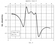
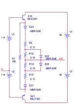
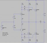
I have found the CCDA & Class-AC article and did some modelling and optimisation. A pair of diodes were added in series of emitter resistors to do the actual switching and a resistor to keep transistors open all the time. See attached schematic. Ib is 1A.
Diodes improve Gm curve. I suppose it is due to similar (identical) switching characteristic of all four elements. Furthermore, together with the bypass resistor they might improve switching characteristic compared to switching transistors at higher speeds.
Optimisation goal was to get as constant Gm as possible. Figure below shows a Gm staying within 4.1..5 in -8..8A range. At -2A and 2A a transition between class A and C happens. Visible asymmetry is due to transistor differences. Asymmetrical resistors would help to straighten it as modelling shows.
Has anyone tried something like this? I am considering this as a possible improvement in some of my burnt class AB amplifiers that are waiting to be fixed.
Attachments
Member
Joined 2009
Paid Member
Looks interesting. I know Wavebourn likes Class AC too and he's built a lot of good amplifiers.
I think it would be worth your effort to try it out. I would start with the simplest implementation first, even if the simulations show it can be improved on. I suspect that the improvements won't be so important in practice.
I think it would be worth your effort to try it out. I would start with the simplest implementation first, even if the simulations show it can be improved on. I suspect that the improvements won't be so important in practice.
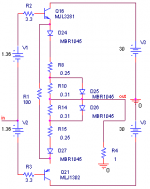
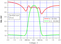
I did some more optimisation. Now Ib=580 mA.
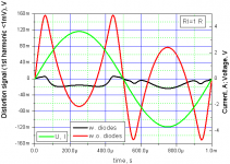
Schematic with diodes shown.
w.o. diodes is a variant without D25, D26,everything else same.
In graphs you can see distortion signals @ 1 ohm load and dynamic transconductance of stages w. and w.o. bypass diodes.
Looking at these results, benefit of adding diodes is clear. As a side effect at increased currents diodes slightly reduce voltage drop thus increasing dynamic range.
I wonder how things will be when temperature comes in in real circuit.
Attachments
With class-ac I have also experimented. With the original circuit I did not become warm.
I then designed the following circuit with Mosfets which also works in class-ac. I've built an amplifier that works very well (Bemos on my private site).
Unfortunately, I do not know how to simulate Gm with LT spice. Perhaps one of you can help me.
I then designed the following circuit with Mosfets which also works in class-ac. I've built an amplifier that works very well (Bemos on my private site).
Unfortunately, I do not know how to simulate Gm with LT spice. Perhaps one of you can help me.
Attachments
Member
Joined 2009
Paid Member
I wonder if it would benefit if you turned this into a CFP output - just return the drains of the MOSFETs to the emitter of the input devices above the 1 Ohm emitter resistors instead of directly to the output - reducing the resistance of the 1 Ohm emitter resistors to something around 0.2 Ohm at the same time. This creates a feedback loop though which may not be what you wanted.
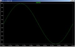
load amplifier with 0R (0V voltage source) VloadUnfortunately, I do not know how to simulate Gm with LT spice. Perhaps one of you can help me.
drive amplifier with DC sweep
Trace d(I(Vload)) and you will get the dynamic output transconductance.
In general, trace would look like
Code:
d(I(Vload))/d(V(in))This is based on a definition of dynamic transconductance:
Gm = d(I)/d(V)
- Status
- Not open for further replies.
- Home
- Amplifiers
- Solid State
- Class AC