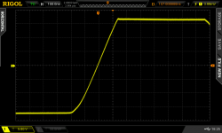
Here is a little toy that I built a few months ago. Slew rate is > 110 volts/microsecond. If you search the site you can find an amplifier by Winfield Hill of Harvard (co-author of the famous book "The Art Of Electronics") whose slew rate is 1000 volts/microsecond.
Attachments
Class AB amps don't typically swing the whole power supply voltage. My PV-1.3k maxes out 600 W 4 ohms or 49 Vrms, or 68 Vpp from +-85 v power supplies. That would be a 170 v single supply so the swing is 40%. That amp specs 20 V/microsec slew rate. That is for <-.1% Harmonic Distortion. They sold thousands of them in the PA market.All,
What would folks consider to be an acceptable slew rate? By my calculations, If I were to use this at the full 65V supply voltage, I would need a slew rate of at least 8.2V/us for a full 65V swing at 20kHz (2*PI*20,000*65/1,000,000=8.164).
If you've got a stash of TIP102/107 in your drawer, cool, but TIP142/142 are TO247 in stead of TO220 and have 1 deg C/W rating instead of 1.5 deg C/W of the former. The latter cost me $1.12 each.
If you've got power limitation in your BC556 TO92 limiting the current, try MPSW56 from ON with the 1 watt case. Or 2n6716/2n6727 from Zetex/Diodesinc also in a 1 watt case.
**** your sim in post 15 shows 48 v single supply. Now you tell me it is calculated for 65? 65 might be pushing it on TIP102 that leaks 30 ma @ 100 v, the Vceosus rating.
I've got a 20 amp 48v regulated Lamda supply surplus in the attic. 65 v would be some import **** toroid from the country that last year built new islands near the oil fields off their neighbor's coast & this year banned beards in some province.
Last edited:
Class AB amps don't typically swing the whole power supply voltage. My PV-1.3k maxes out 600 W 4 ohms or 49 Vrms, or 68 Vpp from +-85 v power supplies. That would be a 170 v single supply so the swing is 40%. That amp specs 20 V/microsec slew rate. That is for <-.1% Harmonic Distortion. They sold thousands of them in the PA market.
If you've got a stash of TIP102/107 in your drawer, cool, but TIP142/142 are TO247 in stead of TO220 and have 1 deg C/W rating instead of 1.5 deg C/W of the former. The latter cost me $1.12 each.
If you've got power limitation in your BC556 TO92 limiting the current, try MPSW56 from ON with the 1 watt case. Or 2n6716/2n6727 from Zetex/Diodesinc also in a 1 watt case.
**** your sim in post 15 shows 48 v single supply. Now you tell me it is calculated for 65? 65 might be pushing it on TIP102 that leaks 30 ma @ 100 v, the Vceosus rating.
I've got a 20 amp 48v regulated Lamda supply surplus in the attic. 65 v would be some import **** toroid from the country that last year built new islands near the oil fields off their neighbor's coast & this year banned beards in some province.
Yeah, I guess assuming the full voltage swing is being somewhat conservative. My simulations indicate that this design should have a voltage swing of about 57Vpp for a 65V supply voltage and an 8 Ohm load, and and about 41Vpp for a 48V supply (53Vpp and 38Vpp respectively for a 4 Ohm load). I intentionally designed for a Sziklai pair configuration on the power stage to help maximize the voltage swing at the output
As stated in the first post, simulations were done for a 48V nominal supply voltage (most likely a cheap, noisy switching supply, hence the desire for the constant current biasing), but I wished to design the amp to work over a supply range of 36-65V, as I may do several experiments using this design. 65V was given as the maximum simply because that is the maximum rated voltage of the BC546/556.
TIP102/7 was chosen simply due to availability and cost. Thanks to it's popularity with hobbyists and microcontroller enthusiasts, one can buy cheap bulk lots of 50 or 100 on Ebay for under $0.20 per piece. I didn't know about TIP142, so that's definitely good to know
Thanks to the high current gain in the power stage and the low quiescent current in the amplification and differential stage, the average power dissipation in the BC556 transistors should be no higher than about 90mW even for the worst-case 65V supply voltage, so no worries there.
Last edited:
Well, cool that the CCS's can cope with 48 or 65 or whatever supply.
I really like the single supply/output capacitor design, for protection of my $300 ea speakers with only one part per channel. Most designs with this feature were designed about 1966-78. Just dumping the quasi-comp output transistors is a giant step forward for single supply.
Also $1.12 each for TIP142/147 from newark is a wholly more attractive category of experiment from those $5 each 2SC5200/2SA1943 the majority are so enamored with. The Fairchild versions we can buy here may not have the flat gain/current curve that the Europeans are always bragging about.
I might build one of these next - the honeybadger etc and most other designs discussed here have the easyflame speaker feature - direct coupled output transistors. One solder joint failed, boom, DC on speaker. I don't wave solder my experiments, I mess them up by hand. Good mosfet protection circuits are about 20 parts.
I'll be watching to see if you come up with an artwork I could xerox on a photoetch board. It is a bit too many wires to hand build.
If you decide to up the quantity of your board purchase, do link to a group buy thread, I might be interested. 4.75" x 10" is the max dimension in my salvage motor drive enclosures if the OT's line up on the back heat sink, and the two boards stack, if that is convenient for you.
You might put a centering resistor or pot to put the middle point right at 1/2 the supply. Most transistors are not that matching. I'd be using MPS8099 NPN MPSW56 PNP for first trial since I have over 100 of each at about $.08 genuine ON Semi.
Last edited:
Just use a decent soundcard (something like a Xonar D1/DX should be quite sufficient) and wire up an output attenuator of 20k/1k or so. Mind the inherent ground loop, a 1k or so between output GND and line-in GND may prove helpful. Plan B, have one end on a battery-operated machine.What is the recommended method for measuring THD for a real amplifier? I have an HP 334A distortion meter, but it's only rated to a minimum of 0.1% THD. I also have a crusty old HP 141T/8556A spectrum analyzer/tracking generator mainframe, which I think may be my better option, but even then I don't know if I have a sine wave source with low enough distortion for accurate testing...
Advanced techniques are available for more sensitive measurements (notch filters, bridge approach).
I'll be watching to see if you come up with an artwork I could xerox on a photoetch board. It is a bit too many wires to hand build.
If you decide to up the quantity of your board purchase, do link to a group buy thread, I might be interested. 4.75" x 10" is the max dimension in my salvage motor drive enclosures if the OT's line up on the back heat sink, and the two boards stack, if that is convenient for you.
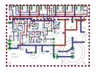
I have finished with a first draft of the PCB layout. I am also trying to work on a breadboard prototype in parallel, but I may end up breaking down and ordering the boards to make the prototype instead.
The board comes in at about 3"x4" (10x7.6 cm). It is unlikely that they would stack easily, as the large C8 capacitor is about 50mm tall. I tried to make the layout pretty dense. It's double-sided, so it may be difficult to do hand-etched boards of these.
I'm pretty new when it comes to PCB layout, so let me know if there is anything I can do to improve/correct my board layout. Should I be putting the pads for the power transistors right against the edge of the board, or would it make sense to pull them back a bit?
Attachments
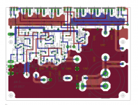
I'd say output transistor pads along edge is traditional.
those long parallel runs between base & collector of output transistors might cause oscillation. I'd be tempted to fly in the bases in the third dimension.
You need to put a resistor pads between base of Q12 and plus & minus rails to allow for centering the output to the speaker capacitor. This won't show up in simulation, transistors are symmetrical in sims. But centering the output would eliminate one sided clipping due to inadequate headroom one way or the other.
There may alternately be something you can do at the connection of Q5 and Q7 to do the centering, for less current, but I'm not experienced enough with CCS to know exactly what to do there.
With 50 cm tall output cap I could cram 4 of these in my motor drive chassis. Heat sink is 7" x 5" along the back.
PM me a price & surface mail address I'll send MO for a couple of boards.
Last edited:
I'd say output transistor pads along edge is traditional.
those long parallel runs between base & collector of output transistors might cause oscillation. I'd be tempted to fly in the bases in the third dimension.
You need to put a resistor pads between base of Q12 and plus & minus rails to allow for centering the output to the speaker capacitor. This won't show up in simulation, transistors are symmetrical in sims. But centering the output would eliminate one sided clipping due to inadequate headroom one way or the other.
There may alternately be something you can do at the connection of Q5 and Q7 to do the centering, for less current, but I'm not experienced enough with CCS to know exactly what to do there.
With 50 cm tall output cap I could cram 4 of these in my motor drive chassis. Heat sink is 7" x 5" along the back.
PM me a price & surface mail address I'll send MO for a couple of boards.
I doubt that there will be significant capacitive coupling on the PCB. The internal Cob of a TIP102/7 is like 200/300pF already anyway. Or is that not what you meant?
I'm not sure I understand what you mean here. The center point will be set using the R5 trimmer on the input bias CCS. I use R2 in combination with the CCS to set the center voltage. I have done this on past designs and had no issues. Even in the simulation, the clipping levels are slightly asymmetrical.
I'll PM you about the boards, although you may want to wait until I've actually tested it before you offer to buy any. 😀
Okay super, I don't understand CCS enough yet to understand what R5 was doing to Q2. Centering figured out already, great.
1.5 mH on output inductor is traditionally a solid core wire wrapped 12 turns around a china marker. Peavey calls that 0.8 mH. Size can be TBD, even stood on end. 22 ga wire should be good enough for this power rating. I have a coupla rolls of that.
As far as RF coupling between long parallel runs, it is not so much capacitance I don't believe. More of an inductance. Happens in the RF where you don't want the output transistor burning up current while it oscillates. 8 pf an inch isn't a bare wire in open air?
Usually amp boards have 3 amp diodes between the output and the rails. this could be outside (field side) the speaker cap. this protects from induction voltage spike if the speaker wire comes loose under high currents. These diodes are usually back biased.
I've cut & spliced PC boards in checkout professionally, I don't expect them to be perfect first time. All that CCS stuff in TO92 in the front end I'd like printed out, wiring that by hand would be tedious. For a look at my board & wire construction technique you may look at this: http://www.diyaudio.com/forums/solid-state/236256-retro-amp-50w-single-supply-20.html
Crude but doesn't oscillate overheat hiss or distort (much) .
Connections are loops of wire through 2 holes on board at the edge. on board wires solder through the loop, field wires solder through the loop. No funny little Euro connectors to buy.
If you up the buy from 3 quantity boards to 5 or 6 maybe price each will drop.
Have fun.
More info. If you learned electronics in the northern hemisphere, you probably used 2n2222/pn2222 in your lab course. BC556/546 from Motorola/ON have the opposite pinout, with the flat pointed at you, CBE, so the flat goes backwards on the artwork if one is using something normal like MPSA06/56 or MPS8098/8099. Datasheet BC546 from Phillips (which one can't buy in US) are EBC. Which pinout jiny used for the artwork is TBD.
As stated in a PM, power goes in on TP1 & TP2.
TIP102/107 are $.38 each from ST at Newark today, but if one wants to avoid the $5 freight, TIP41c/42c should fit with about .8 A soa @ 50 v. Q11 vbe multiplier would be turned down for 2 junctions. R15 is set for 2.6 ma on the VAS stack, so if Q14/15 have about 20 gain & Q15/18 are the same, then *400 gets 1 amp out. 8 W on a speaker. But if you decrease R15 to 120, then *400 gets 2.56 amps out, which is about the soa of three TIP41/42c parallel @ 50v. 52 W.
Very useful board for experiments with CCS/LTP plus an output capacitor to save the speaker with only 1 part/channel.
Note TIP102/107 have a back voltage flywheel diode, TIP41/42 does not. However to protect the output capacitor C8 against back voltage from speaker disconnects or ringing, back diodes to the power supplies need to be put external to C8 anyway.
Last edited:
I used a CBE pinout for the PCB layout. I chose BC546 over a 2N-series BJT simply due to the slightly higher 65V max Vce rating versus the 40-50V ratings of most 2N types like 2N2222A/2907A or 2N3904/3906. I may also experiment with the 140V-rated 2N5551/5401 pair, which would allow for supply voltages up to 100V with modified values/power ratings for R2, R3, R6, and R14 so that they don't overheat. Thanks to the heavily constant-current controlled biasing, the stability margins and slew rate are pretty much independent of supply voltage.
The issue of current limiting in the power stage if a non-darlington pair such as TIP41C is used makes sense. It might be possible to raise the quiescent current in the VAS stage or bin the MJE340/350s and/or power transistors for higher than average gain, but you still run the risk of the output current topping out and causing the amplifier to clip early.
I also updated my pspice model to use more accurate transistor models from Onsemi's website rather than using the stock 2n3904 models and the darbreakP model. resimulation didn't show massively different results, but I increased R8 and R9 to 470 to help improve the simulated stability margins and distortion. The real best value to use may have to be determined experimentally, or may depend on the gain of the transistors. I plan on using BC546B gain-binned transistors.
I have put in an order for several prototype boards, so I will give updates when those arrive.
Last edited:
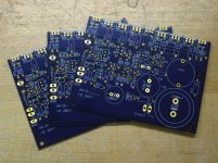
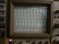
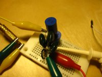
I have finished building the initial prototype and begun testing. Everything seems to be working correctly and seems relatively stable.
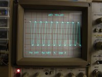
Slew rate was roughly measured at approximately 6V/us, which is lower than anticipated. looking back at my simulation, I think I may have set up my simulation incorrectly by having an input signal that was over-driving the output. resimulating it with better values comes out to a slew rate of about 7-8 V/us. Hmm...
Maximum output swing is measured at about 41Vpp for a +48V supply, which comes to about 26Wrms max output. This is pretty much exactly as per the simulation values.
I will be setting up for distortion measurements next, but as stated previously, I need to check if my cheap signal generator is low enough distortion for precise measurement. I recently ordered a Keithley 2015 THD multimeter, so I may have to use that instead when it arrives.
Attachments

Last edited:
Great. 26 vac out of 48 rail is very good. What load was that, 8 ohm? Speakers or resistors?Slew rate was roughly measured at approximately 6V/us, which is lower than anticipated. looking back at my simulation, I think I may have set up my simulation incorrectly by having an input signal that was over-driving the output. resimulating it with better values comes out to a slew rate of about 7-8 V/us. Hmm...
Maximum output swing is measured at about 41Vpp for a +48V supply, which comes to about 26Wrms max output. This is pretty much exactly as per the simulation values.
Even no errors found and no oscillation is also better than expected.
The load is a large 6 Ohm speaker, albeit on a somewhat long cable. I initially powered it up open circuit and did not see any signs of instability, either.
Last edited:
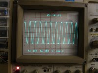
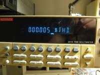
My new THD meter came in. It turns out the cheap signal generator I was using had a THD of around 0.3%. Good enough for basic testing, but nowhere near clean enough for THD measurement. Fortunately, the THD meter I got comes with its own signal generator on the back.
Initially, I also had some trouble with the Keithley 2015 because its own signal source was measuring about 0.028% THD just by itself, which is out of spec if I read the manual correctly (I guess that's what I get for buying "refurbished" equipment on ebay). However, after cobbling together a quick 1kHz low-pass filter to put in line with the signal source output, I was able to bring that number down to about 0.004%, which, if I understand correctly, is roughly what the device is rated for in the manual.
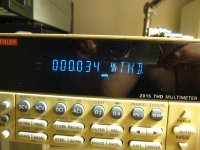
Measuring for a 1kHz input signal at about 1Vrms output and about 50-75mA bias current per pair (the bias current fluctuates a fair amount with temperature), I measured about 0.005% THD at the output, which is effectively in the noise floor of the instrument. Raising the output level to about 10Vrms at the output caused the THD to increase to about 0.034%.
Overall, I would say I am fairly happy with these results, although correctly simulating and designing for better slew rate will be high on my priorities list for future designs. This is the first time I have really done detailed measurements on one of my designs, so I don't really have a reference point for whether these are good results or not. I have seen a fair amount about simulated numbers, but I have not seen as much in the way of physical measurements for comparison.
Initially, I also had some trouble with the Keithley 2015 because its own signal source was measuring about 0.028% THD just by itself, which is out of spec if I read the manual correctly (I guess that's what I get for buying "refurbished" equipment on ebay). However, after cobbling together a quick 1kHz low-pass filter to put in line with the signal source output, I was able to bring that number down to about 0.004%, which, if I understand correctly, is roughly what the device is rated for in the manual.
Measuring for a 1kHz input signal at about 1Vrms output and about 50-75mA bias current per pair (the bias current fluctuates a fair amount with temperature), I measured about 0.005% THD at the output, which is effectively in the noise floor of the instrument. Raising the output level to about 10Vrms at the output caused the THD to increase to about 0.034%.
Overall, I would say I am fairly happy with these results, although correctly simulating and designing for better slew rate will be high on my priorities list for future designs. This is the first time I have really done detailed measurements on one of my designs, so I don't really have a reference point for whether these are good results or not. I have seen a fair amount about simulated numbers, but I have not seen as much in the way of physical measurements for comparison.
Attachments
Looks good but one question? Why a single rail AC coupled design in this day and age? Are you running from a 48vdc power source?
Note that mot enterprise class IT and communications gear can operate from 48 volts which is a by product of the telephone company. Just note that's the standard is -48v with a positive ground.
Note that mot enterprise class IT and communications gear can operate from 48 volts which is a by product of the telephone company. Just note that's the standard is -48v with a positive ground.
Yes. This design is primarily meant for use with a single-rail 48Vdc switching supply.
I'm not sure, but I think I could reverse the design for a positive ground if needed by swapping all the NPNs for PNPs and flipping all the capacitor polarities. I don't even think I would need to change my board layout.
I'm not sure, but I think I could reverse the design for a positive ground if needed by swapping all the NPNs for PNPs and flipping all the capacitor polarities. I don't even think I would need to change my board layout.
Because great speakers cost $600 each up, amp boards cost $50 loaded. Serious DC rated protection relays (tungsten parallel silver contacts) cost $$ and ship from Europe. Protection mosfet circuits have more parts than the amp often. Assembled mosfet board ship from countries we are at war with or that transfered all our consumer electronics jobs to serfs.Looks good but one question? Why a single rail AC coupled design in this day and age? Are you running from a 48vdc power source?
Speaker caps cost $3 , can be bought made in USA, and have been tested effective in a flaming amp situation by this purchaser. The speakers are fine, still in use. The 99.9999% of you posters that subject your speakers to direct coupled transistors might have tin ears. This board could possibly replace an AX6 which is okay so far but not amazingly good. Fully complementary output speaker cap amp designs development seemingly stopped in 1980, except for this. Big mega-corporations ring up profits when you flame your speakers at the same time as the amp.
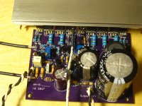
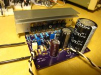
Received the boards this PM, thanks jlny. Tsistor Pads are so tiny I will have to purchase a better soldering iron before I assemble, IMHO. have a great summer.
Congratulations on the distortion measurements.
Off to practice my Sohmer console which has 88 keys of beautiful full frequency sound. Hope this board sounds close some day.
Last edited:
Glad to hear the boards arrived. Thanks, I'm pretty happy with the results.
Also, yes, some of the pads are a bit small. Those are the default pad sizes used in Eagle, so I may have to go in and edit the pad layouts if I want to make my designs a bit more hobbyist-friendly. I'm still relatively new to using it.
As for a soldering iron, I just use a generic "937D+" soldering station clone with a pencil tip. Soldering stations like that can be had on ebay for maybe $30, and they are decently good for what they are. Just be sure to check for the occasional shoddy unconnected ground wire...
My only other comments would be to be careful on the pads that connect directly into the ground planes-- it will take quite a bit of heat to get good joints on those and my relatively weak iron had some trouble delivering enough heat. Before powering up, I would recommend setting R17 to its maximum resistance so that the bias current will be zero at the initial startup. For a 48V supply, R5 should be set to about 142 Ohms for initial startup and adjusted as needed for VCC/2 at the output behind the output capacitor.
- Status
- Not open for further replies.
- Home
- Amplifiers
- Solid State
- Class AB amp using TIP102. Seeking Critique