I just had an idea on how to get class A performance using a class B or AB output stage.
Start with a class A, dual Mosfet, P-P output stage (or could be tube, but won't save much power then), then cascode above that into two tube cathodes. Then the tube plates drive the P-P OT. So one has class A type currents coming into the tube cathodes. Nothing unusual so far, would be class A P-P operation.
Next, put a gyrator type CCS load on each (top cascode) cathode to absorb the class A idle current or most of it. What is left is the class B or AB currents going through the tubes. Use the gyrator adjustment level to fine tune the class A null to leave class AB or class B operation topside. Ie, adjust for no crossover notch and a little class A current overlap for the top devices. Bottom devices still operating in class A.
Local plate feedbacks to the previous driver stage would be needed to lower the output Z.
Some fast clamp diodes on the tube cathodes could be used to set a cutoff level just above minimum conduction level, minimizing turn-on time/or capacitance charging effects.
One could do 3rd harmonic null with a tail resistor, or a CCS tail on the bottom Mosfets if wanted too. With 3rd harmonic nulled out in the class A section, the reduced class AB or B currents topside should be lacking 3rd harmonic too. Similar for higher odd harmonics if nulled bottomside. (the Gyrators are just removing the class A DC idle current from each side)
Well, just an idea. I'm too cheap to pay for class A heat, so I'm demanding the class AB or B output perform as well as class A.
One could even put a servo in to control the gyrator levels. It would monitor the B+ OT lead for minimum current level and control the gyrators to maintain that.
Another servo could be used to monitor the individual minimum tube currents and adjust their grid bias for DC balance. Basically a conventional class AB bias control. Or just put a bias pot on one of the grids for manual balance adjust.
One could also flip it around and use tubes on the bottom with low plate voltage, and Mosfets above for the cascodes. Wouldn't save as much heat that way.
Could also use the secondary (0,4,16 Ohm taps) for a CFB winding for the class A Mosfets (bottom stage, put 0 and 16 Ohm terminals under the sources and 4 Ohm terminal to ground) if wanted.
Last edited:
No comments? It's not April 1st.
A simple synopsis:
Build a class A, P-P output stage with cascode tubes on top to drive the P-P OT.
Then add some CCS's to the cathodes of the top tubes to draw off 95% of the bottom stage's class A idle current. So the top tubes are left with class aB currents. But they are identical to the bottom class A (AC) currents during their ON cycle. A fast diode clamp gets added to the cathodes also, to prevent them from quite turning off during the OFF cycle for each tube (top side).
What's different from class aB? Normal class aB is voltage driven on the grids, so has V to I transfer curve distortions (low gm) around the low current regions. Plus significant issues with getting the two tube currents to add up seamlessly without crossover distortion.
While this scheme is current driven through the cathodes with the class A currents -CCS currents. Current in = current out. That's the key. Must give identical results to class A, since the DC through the OT does nothing.
The top tubes are held in a slightly conducting state during each (class B) cut-off phase portion to prevent switch-on time or capacitance charging effects. The (class A -CCS) current just lifts the cathodes off the minimum conduction point to go to it when needed.
As far as I'm concerned, normal class A is history, no more heat needed.........................
Maybe I should call it the "DC Stripper", that'll get some attention!
Last edited:
True. But pentode outputs have the same issue. Just use some local N feedback (final plate R's) back to the class A grids or back to the previous driver stage. Or put CFB (could be just the secondary, 0,4,16 OHM) into the "cathodes" of the bottom class A stage.
How do you ensure that the two CCS run identical currents, so the switching point is the same for both sides? If not, bad crossover.
The junction points will have distorted voltage signals (in order to switch off (almost) the upper devices), so harmonics will be generated. OK, provided that the two points have the same stray capacitance so things remain matched at ultrasonic frequencies. If not, bad crossover.
The CCS will dissipate some power, although less than a full Class A circuit. You will need a separate supply rail for them.
My gut feeling is that if it was that easy to get Class A performance at Class B efficiency then everyone would be doing. Most 'bright' ideas turn out to have some major snag; just a few are actually workable.
I'll try to get an image up sometime tomorrow. Nothing here to draw with.
It's just a class A P-P stage with "grounded" grid cascodes above. Then add a CCS load on each side of the cascode cathodes to draw off most of the bottom stage class A DC idle current. The diode clamps are just final touches for ultra smooth operation.
I had to think about the CCS matching a bit, and looks like that will need precision matching and precision 180 degree cutoff too, since it determines how much AC signal portion remains on each top side. The DC component itself only makes for a slight DC imbalance in the OT.
Oh well, another neat idea bites the dust.
Last edited:
It's back from the dead.
The "DC Stripper" is back on the prowl:
Turns out it's not so hard to fix the balance issue. When the currents are matched, the clamp diodes must be sinking the exact same AC current as the opposite top side cascode tube absorbs at its cathode. So two small differential current xfmrs get put in to find the difference in those currents (one for each side). Then since the two sides must also match, one connects them together with a tertiary winding, but flipped. The error difference on one side provides the error correction signal for the opposite side, and visa- versa. Ie, they self null the errors. Then a nice simplification arises, both differential current xfmrs can just be put on the same core with all four windings on it.
So the differential current error xfmr fixes the balance as long as the error voltage (from Verr= Ierr* xL) can be supported across the diffl. xfmr. And then, one can just go and adjust one of the top CCS (DC strippers) so that the differential xfmr has a null voltage on it, so it has essentially nothing to do. The diffl current error xfmr then takes care of any drift due to tube aging or CCS stripper drift, but one may still want to null it occasionally to prevent any magnetizing current (from the error voltage on the core) in the diffl. current xfmr causing a small distortion issue.
I'll definitely have to get a diagram up now. But I want to do some simulation or actual testing on it first to verify this is all working, getting into mind boggling territory now. Although the implementation is fairly straightforward. The computer here cannot do much (no hard drive space left), so I will have to get something else.
Last edited:
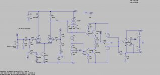
Here is a rough schematic of the DC_stripper. (or class A without the heat)
It essentially derives class A currents below, at low voltage, then strips the idle currents off, to leave class B operation for the top devices (at good efficiency). Advantages over usual class AB are that it maintains constant total gm across the full signal window, and eliminates crossover distortion (no total gm variation, instantaneous sub-uSec simultaneous crossover).
Q1 and Q2 operate in class A mode to derive the drive currents for the tubes V1, V2 (or Mosfets) above. The gyrators remove the class A idle currents, leaving just the AC signal. Negative excursions of the AC signal operate a valve, V1 or V2, while positive excursions of the AC signal get absorbed by the clamp diodes D1, D2.
The Rc resistors are there to symmetrize the loading, they are set to emulate the upper cathode input impedances, so the AC sees a constant impedance regardless of polarity. This symmetrizing is needed to avoid voltage drift of the gyrators when signal is present. (V_idle just needs to stay within a window, precise matching for side to side does not matter)
The gyrators (controlled CCS's) adjust their current to exactly match the idle current of the lower Q1 or Q2. The cathode/gyrator idle voltages are controlled just below (ie, + above cathode actually) tube conduction threshold (Vadj on each side sets the idle voltage) and below clamp diode conduction. (ie, both V_idles set in a narrow voltage window between tube conduction and clamp conduction)
Whenever the current from lower Q1 and Q2 varies (complementary fashion due to the class A CCS'd drive), it immediately swings to either tube conduction or diode conduction. This is because the imbalance in opposing currents from the Q below and the Gyrators above "instantly" swings to tube or diode clamp conduction. (ie, battling current sources into near infinite load impedances within the window)
Since both sides are maintained in the small idle windows by the gyrators (just between tube conduction and diode conduction), and the class A stage below performs exactly complementary current operations, the switch from tube conduction to diode clamp conduction is immediate and simultaneous for both sides. (sub uSec, depending on distributed capacitance)
There still remains the possibility that one side has more AC current sent thru, but this is determined by the balance of the lower class A stage balance. This is no different from a normal class A situation. Q1 gate bias can be adjusted to match DC (and hence AC gains). Or, a servo could be used with a dual CCS tail (cap coupled across) to exactly match currents (for say a toroid OT).
Some details, like grid/gate input resistors and ground plane bypass caps for critical reference voltages are not shown. Low distributed capacitance around the Q1,2 drains/D1,2 anodes/Gyrator outputs/tube cathodes is essential for ultra fast operation of conduction switch-over.
Attachments
Last edited:
Woops, minor correction.
DC imbalance on the bottom class A drives actually doesn't cause a problem up top.
(and a normal class A P-P could only have DC imbalance with a CCS tail, no AC gain mismatch issue anyway)
The reason is that the topside Gyrators will remove any DC, whether from balanced or unbalanced class A below (ie, whatever it takes for the Gyrator to get its idle voltage requirement).
Balancing the bottom class A section (bias adj) though, will provide a bit more AC signal headroom.
Now a super simple approach to low power (in the tubes anyway) class A.
This just uses a Mosfet regulator to keep the plate voltage near constant (and low) on the conducting tube by raising the B+ only when needed. The tubes are operated in conventional class A bias. This might work for triodes too, but they will be operating with near constant plate voltage like a pentode (ie, screen grid). (the Mosfet effectively operates class A if the tubes are in class A, but the tubes can be set up for any amount of class AB and the Mosfet follows suit.)
This would also work well for class AB on the tubes, if you want to keep their dissipation down. (the Mosfet still gets class AB hot too though)
A switching regulator could be used instead of the Mosfet regulator to control B+, to get efficiency in class A (tubes) for the regulator too.
Attachments
Last edited:
DC_stripper upgrade:
The clamp diodes D1,Rc/D2,Rc in the DC_stripper circuit above need to match the impedance of the tube cathodes, otherwise large AC (audio) signal +/- polarity loading differences could cause drift of the DC Gyrator Voltage setpoints. (any drift of the Gyrator/cathode DC voltage out of the Hi Z window would cause transient crossover problems)
The original Diode/resistor combo is only an approximate match to a tube cathode, due to it's varying gm with current. So a better clamp is shown attached here, which can be made to follow a power law up to 2.0 by proper choice of resistors. Low R3 gives near 2.0 power law, and higher R3 gives closer to linear 1.0 power law. The tube cathode will probably be near 2.0 power law, so R3 will probably want to be 0 Ohms.
Attachments
Last edited:
Interesting idea. I have a similar idea already drawn with an LTP output stage with mosfet mu followers above the triodes. Waiting for real life verification though...
re: Ballpencil
The floating supply, class A follower, output stage with a class AB rail driver is a classic approach. I assume the OPA541 is a power Op. Amp. I forget who had the patent on that approach long ago. Technics?
I have tried to find a tube equivalent, but the sum of currents at the center tap of the usual P-P OT is in the wrong form to do it. Need the difference. One has to drive a differential power source through another OT then, not too attractive then.
One can just put a small class A tube amp OT secondary in series with a class AB high power amp (with a very low Zout secondary, like 0.2 Ohm for the class A tube amp) and then take the global feedback (for the class A amp) from the sum point. The class AB amp essentially drives tracking B+'s back through the class A OT. With the right turns ratio in the class A OT and the right gain distribution between the class A and class AB amps, the class A tubes can sit with near constant voltage across them (even though they are conductance modulating).
Last edited:
The "DC-Stripper" approach above is mainly a simulation exercise, proof that it is possible, but not real practical, unless the DIYer enjoys tweaking a bunch of touchy adjustments with a scope attached. No commercial prospects whatsoever. But that can be an attractive DIY prospect sometimes. (climbing Mt Everest....)
----------------------
Another, far more practical, approach is to use differential current local feedbacks on a class AB output stage. This ensures a constant I out per V in, making gm constant and Zout constant, but finite. Global NFDBK can then lower the Zout further and increase the effective gm. This approach has the interesting effect of pre-distorting the drives to the class AB stage, to make them perform as class A, but at the lower power dissipation of class AB. (Note: Differential current (between the output devices) is the same as the output current.)
(it is easily implemented for tubes by just putting a couple of current sense resistors in the cathodes of the class AB output stage and feeding the NFDBK signals back to a high gain differential driver stage.)
Here is a SS version mentioned by Broskie, helpful for imagining what happens with the local Neg. feedback during crossover.
European Triode Festival and Crossover Notch Distortion and New OTL Design
Attachments
Last edited:
re: Pauldune
"I have a similar idea already drawn with an LTP output stage with mosfet mu followers above the triodes."
You probably need something like this:
The two OTs need to be separate if you want just the class A part driving the output unfortunately.
"I have a similar idea already drawn with an LTP output stage with mosfet mu followers above the triodes."
You probably need something like this:
The two OTs need to be separate if you want just the class A part driving the output unfortunately.
Attachments
Last edited:
Here is a schemo for Differential I Neg feedback with local V Neg feedback also. Ratio of V to I feedback sets the local Zout (and the constant gm total for the output stage). Outside Global V Neg Fdbk then lowers the Zout. Top Output stage is operating in class AB, bottom driver stage is operating in class A. The results will look like a class A output, since the total output gm (sum) is held constant.
(The bottom R1's and bottom CCS may not be needed, depending on how the value of Rfdbk_I is set. )
(The bottom R1's and bottom CCS may not be needed, depending on how the value of Rfdbk_I is set. )
Attachments
Last edited:
- Status
- Not open for further replies.
- Home
- Amplifiers
- Tubes / Valves
- Class A output without all the heat cheat