I've been reading up on tube-rectified power supplies and currently working my way through Morgan Jones' excellent book. That said, I'm a little unclear as to the section regarding snubbers on choke input power supplies to help with smoothing. My confusion is purely based on my reading of the diagram and my desire to understand choke input power supplies. The image below depicts a typical snubber approach on the left and an improved snubber on the right.
The way I'm reading it is that that in the improved snubber on the right, the 265 Ohm resistor represents the internal resistance of the choke and NOT an additional resistor. Is that accurate?
A bigger picture question is why don't I see these snubbers in more schematics with choke input power supplies?
Thanks in advance!
Is that not mentioned in the text? Knowing Jones I'm sure he will make that clear.the 265 Ohm resistor represents the internal resistance of the choke and NOT an additional resistor. Is that accurate?
That's why there is all that text holding the pics apart ;-)
Also because not all 20H/120mA chokes will be identical.
Jan
It is mentioned that the improved snubber uses the internal resistance of the choke , so that is clear .
But I don't see the purpose of the second 220nF as the output must be connected to a large electrolytic capacitor anyway .
But I don't see the purpose of the second 220nF as the output must be connected to a large electrolytic capacitor anyway .
Last edited:
Does your copy of the book contain this passage?
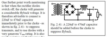
It appears that Dr. Jones's choke has an inductance of 20 henrys, a parasitic series resistance of 265 ohms, and a parasitic self capacitance of 162 pF. Thus the choke's self resonant frequency is 2800 Hertz. A choice of C1 = 220nF is therefore an assumption that the leakage inductance of the mains transformer is approximately 15 millihenrys. (0.015 henrys in parallel with 220nF gives a resonance at 2800 Hertz).
Optimum high frequency filtering is obtained by choosing C1 so that it resonates with the leakage inductance of the mains transformer at the same frequency as the self resonance of the choke.
It appears that Dr. Jones's choke has an inductance of 20 henrys, a parasitic series resistance of 265 ohms, and a parasitic self capacitance of 162 pF. Thus the choke's self resonant frequency is 2800 Hertz. A choice of C1 = 220nF is therefore an assumption that the leakage inductance of the mains transformer is approximately 15 millihenrys. (0.015 henrys in parallel with 220nF gives a resonance at 2800 Hertz).

Snubber is important with sold state rectifiers, not so with tube rectifiers. The ringing of stray power transformer LC is triggered by "strikes", rectifier cut-off at forward voltage. Vacuum rectifiers don' have forward cut-off, so no strikes and no ringing.
Another thing that needs snubbing in a choke input supply is voltage spike at start-up. A small high voltage capacitor or varistor across rectifier output will do the job.
Another thing that needs snubbing in a choke input supply is voltage spike at start-up. A small high voltage capacitor or varistor across rectifier output will do the job.
Perhaps some insight is that the external 20H choke has an impedance that rises from low mains frequency up to a peak value at the first self-resonance of 2.8kHz, where that impedance will be quite high (ie. into the 10-100kohm, so nearly a brick wall to noise and switching frequency around 2.8kHz), but noting that noise or signal at higher frequencies will be easier to pass through as the choke starts to look more like a capacitance (up until the next choke resonance). From the few commercial chokes suitable for valve amp power supply application that I've tested, the first self resonance is typically going to be about a few kHz.
The power transformer secondary winding acts like a series LC at diode turn off, where the L is the winding leakage inductance (and transient energy source), and the C is the self-capacitance of that winding, in parallel with any added external snubber capacitance, as per the process of the Quasimodo test jig for tuning the external snubber values. The self capacitance of the winding would be far less than 220nF, so the 220nF dominates as the resonant cap and is the loop taken by transient resonant current.
But to backtrack, Morgan starts by presenting a voltage waveform at the choke input showing the disturbance due to the rapid diode commutation forced by a choke input filter - which is accentuated for plot viewing by having no output load. That disturbance ringing is at circa 890Hz and would be the power transformer leakage inductance ringing its energy out through the shunt capacitance of the PT winding and the unloaded choke capacitance, which is discussed as being heavily damped when load current flows.
Imho, a key point is to use fast ss rectifier diodes such as UF4007 rather than 1N4007 for such choke-input configurations, given that this issue was effectively non-existent when only valve rectifiers were in use. Another key point is to add a bypass cap, such as 220nF, so that disturbance current from the power transformer winding is shunted back to the winding (via CT) with minimal loop area. A related aspect is that a C-RC snubber(as per Quasimodo style) directly across each power transformer secondary half-winding would likely be the better way to constrain transient energy to the smallest local loop around the offending portion of the power transformer (ie. rather than using a restraint that is further afield like the 220nF shunt before the choke).
I'd view the second 220nF cap on the output of the choke as a way to again manage any residual ringing current to just the local circuit, rather than let it pass further afield to wherever the main e-cap filter is (which is perhaps why Morgan made the point of that cap connecting to the CT node).
Have a look on utube, Mr Carlsons lab 6 pack, this demonstrates the problem described in the book and a solution
which is a 0.47uF cap across the inlet of the chock.
which is a 0.47uF cap across the inlet of the chock.
I note that the choke input voltage ringing at diode commutation was about 30kHz in the 2nd video on the Six Pac by Carlson.
I would caution that it may not have been the 30kHz 'ringing' that was the main contributor of the audible hum that led to that issue being investigated further. It may have mainly been due to the rapid change in voltage waveform during the region of diode commutation causing magneto-restriction in the choke laminations, as the added capacitance has a major effect on the rapid changes of that waveform.
Pity Carlson didn't swap out the 1N5408's for UF5408's for a comparison, as that may have suppressed the 30kHz ringing, but retained the rapid changes in waveform.
Not all choke input power supplies have problems.
Fix the ones with problems, leave the working ones alone.
Using a small capacitor at the input of a choke input supply, and a large capacitor after the choke can be a problem.
Suppose you use a 0.47uF from the rectifier to ground; then to a 3.8H choke, then to a 100uF cap to ground.
The resonance at the junction of the 0.47uF and 3.8H is 119Hz, almost exactly the 120Hz frequency of full wave rectification of 60Hz power mains. Ouch!
Nobody makes a 3.8H choke, but a 4H might be close enough to be a problem. Change the choke Henrys, or change the capacitor's capacitance.
I'm not so sure about those C-L values actually causing a noticeable resonance, even though a calculation may indicate so. I haven't seen any actual results showing amplified ripple aligned with say twice mains frequency. Perhaps a signal being amplified that is at twice mains, and of a suitable phase, could beat with the C-L and its incoming power.
Although PSUD2 has its limitations, I do use it to test for damped resonances from LC filters by using a stepped load current and looking at the load voltage disturbance. In the example of the 0.47uF and 3.8H filter, there was no (or quite minor) damped oscillatory response for a valve rectifier full bridge, but there was a discernible response for a ss diode full bridge, with the response being an overshoot followed by a damped low frequency ring. However the level of overshoot and number of discernible ring cycles were dependent on the choke DCR and the output load level, and at a LC resonance determined by the output bulk filter capacitance, not the 0.47uF input filter capacitance. Of note is that this use of PSUD2 is equivalent to ringing a bell with a knock - its a step disturbance of output current (power) - so not a class A concern per se.
The use of a valve diode rectifier may add significant resistance, compared to the other loop resistances, such that issues may only be discernable for ss rectifier configs.
Correct, the second cap is not needed.But I don't see the purpose of the second 220nF as the output must be connected to a large electrolytic capacitor anyway .
Attachments
Not so simple. The choke inductance varies because of:
-Different core excitation levels, (Vrms and Idc)
-Core losses (varies with frequency)
Unless you are using a low loss, linear choke line nanocrystalline or permalloy, I do not find worth attemtping to calculate precise capacitor values.
For example, the resonant frequency of a HiB cored choke can be much higher than the nanocrystalline part, due to the decrease of effective inductance vs frequency.
Ooof. I completely missed that part... I have the PDF version and with the viewer, page breaks, etc. were confusing... so yes, yes it does have that section. That said - and after reviewing the helpful comments - it seems the resistance in the diagram (265R) is the internal resistance of the choke in that specific example.Does your copy of the book contain this passage?
As I'm still learning, this is a nice take, and appreciate your time in explaining this. Will re-read (and re-read) that section of Morgan Jones' book with notes from the comments in this post.From a simplistic lumped component/model perspective, I see the energy in the leakage inductance can be viewed as a forcing voltage in series with that inductance, with the C then in parallel with the L-source. But yes it is likely just a perspective/modelling aspect.
- Home
- Amplifiers
- Tubes / Valves
- Clarification on Morgan Jones choke input snubber