Hi all,
I've put together this LM317/LM337 CRC filters based PCB to fit in a spot and replace a much simpler zener and pass transistor affair.
It's my first real attempt at putting together a PCB and paying attention to the layout. I've tried to keep the ground thick and straight, take the adjust pin resistors directly to the load output and place the output and adjust capacitors in the right places.
I have also tried to keep some sort of "flow", as it was put to me, in the power and ground traces.
Critiques and correction gratefully accepted. 🙂
Attachments
Last edited:
Thats very nice, keep going.
Very nice <Insert Borat voice>
I'd increase the solder pad size to increase solderabillity.
Cheers,
v4lve
Very nice <Insert Borat voice>
I'd increase the solder pad size to increase solderabillity.
Cheers,
v4lve
Lol, thank you for the hand holding, I appreciate this isn’t exactly high end stuff... 😀
I just wanted to make sure i hadn’t made any howlers before making the circuit a bit more complicated.
I want to add Elvee’s denoiser function, I think I’m going to have to use smaller heat sinks and do without the second pair of RC filter capacitors before the regulator to have enough space to do that however.
I would appreciate some advice on that however. I have made some measurements that seem to indicate that the filter capacitors before the RC filter take the bulk of the ripple voltage and current. This would seem to suggest that given the choice it would be better to have more of a limited amount of capacitance before the RC filter than after, in this case 4400uf-10ohms-2200uf or the other way around?
I also am wondering about the snubber, can I spread it around a bit around the input connector it should I keep the traces as short as possible?
Finally, should I add some sort of bleeder resistor, maybe with a LED, or do they add noise?
Hi,
You can better utilize your PCB area if you use 4 bigger capacitors at the input instead of 8 small ones (C5-C12).
Use a single resistor per rail in the CRC ripple filter (R3-R6). Just make a provision for higher power resistors. The way you implemented it currently is sub-optimal.
LNK1 overlaps with C5 outline. This will lead to problems when you try to assemble your board. To avoid possible connection issues make CT pad (its called center tap for a reason) between the AC1 and AC2 pads and make a wire link straight to the ground bus on the underside of the PCB (one pad before and one after the bridge rectifier outline).
CRC transformer snubber (C1-C4, R1, R2) will be hard to assemble due to partial overlap with the input connector outline. Make some space between the input connector and the bridge rectifier for it.
Move C13, C16 closer to the corresponding regs. Move reverse voltage protection diodes further away from the regs if you need more space for this.
Make sure the heat sinks do not touch even if you plan to use the insulators or insulated regs, just in case...
Regards,
Oleg
I really don't know if my answer will satisfy you or rather get you upset..
Nice Caps you use meaning CAP 1 - 4. I never have seen caps with diagonal Legs..
so you need to manipulate the legs that the cap is straight in the circuit. wouldn't it be easier just to design the tracks straight so you do not need to bend the legs of the CAPS.. I think these are in the range of 0.1uf and may these are just Carbon, Ceramic or Mylar, so the way you place the tracks and the donuts, it looks ugly.
What's about these DIODE after the regulator, are these there to protect the LM's then Ok the way you draw it, if not as protection then get a second pair LM ready ..
But if these are Protectors then the use of D1 and D3 is more than enough.. and honestly I think there is no need of... The current spike which will flow back will not be that much that it destroys these LM.
May at the end of it you will find out that this "much simpler zener and pass transistor affair" is better...
It always depends what comes afterwards..
What's the voltage you are going to regulate, and how much current would the circuit after this draw?
take a look at Rod Elliots website before you build this..
Have a nice time..
Hi,
You can better utilize your ....... insulated regs, just in case...
Regards,
Oleg
Thank you for taking the time Oleg, much appreciated. I chose the smaller capacitors as I had read that paralleled smaller value capacitors have a lower ESR and are hence better for a power supply, than a larger single cap of the same value. I appreciate that at these current levels and voltages, there may well not be enough difference to bother about. There is also the small matter of the 50x 2200uf 50v capacitors I have already bought...😀
The over lap on the component outlines are fine and from experience, my particular wire terminals are smaller than the Diptrace footprints, as are the snubber capacitor outlines for which I'm using ceramic disc types which take up no space at all. The bridge rectifier i am using also seem smaller than it's footprint by a 1mm in every direction. I will space them out a bit more however as it looks messy and running a simulation with a 250mA load ( the probably end use figure) I don't seem to need more than 2200uf after R3/4.
Talking of R3/R4, I think you're right and I have removed one.
Thank you for the tip about placing C13,C16 closer to the regulator, presumably the output caps C14,C15 should stay as close as possible to the output terminals as possible?
Also makes sense on the protection diodes, their placement being a non critical aspect I then surmise.
The heatsinks have been changes to smaller ones, the design above for was for the largest Aavid extruded heatsink possible. This new one is plenty for the current level I am planning on pulling from it and leaves more space for a possible Denoiser sub block.
I really don't know if my answer will satisfy you or rather get you upset....before you build this..
Have a nice time..
Never upset, I'm posting to learn and constructive criticism is gratefully received.
Thank you for taking the time to look over this.
C1-C4 are ordinary ceramic disc type capacitors, I have found that the diagonal pin footprint works quite well with them and they look cool at an angle. 🙂o🙂 )
The idea behind the diodes are indeed protection and are from the TI datasheet and also Rod Elliot's project 5. In fact in the latter there seems to be another pair of diodes directly across the rails to earth as reverse polarity protection but I have left them off as this will be going into a box and not fiddled with.
It will be powered with a 18V CT 25VA transformer, I want 15V at around a quarter of an amp out of it.
I look forward to comparing it with the old PSU, I have a Heathkit signal generator with a similarly simple zener and follower PSU that I am anxious to upgrade the PSU for if I get the hang of this. Probing the PSU rail of that shows it's modulated by the output signal and I understand that a proper feedback regulated supply will much reduce that.
OK good then it makes sense..
Send in some pictures when you finished with it..
So you say you operate it at 15 Volts 0.25 Amps this equals only 3.75Watts.
I think then it should workout just fine..
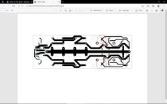
Get this Tracks better connected on Regulator Chips.. *Bigger Red Circle*. Reason is just as easy as this>
if it happens that you need to repair it, exactly there the TRACKS will come off the board after exchanging either one of the Regulators more than one time.
Use good 5 core 60/40 Solder instead this new Machine solder...even it has some lead in it, there is no rule that you have to inhale the fumes of it.. But it is definitely the better solder..
I use Multicore Made in England..
Then also the Circuit has a short circuit drawn *smallest red Circle*on the negative regulator side. check Out the pic..
Good build
Regards Chris
Send in some pictures when you finished with it..
So you say you operate it at 15 Volts 0.25 Amps this equals only 3.75Watts.
I think then it should workout just fine..
Get this Tracks better connected on Regulator Chips.. *Bigger Red Circle*. Reason is just as easy as this>
if it happens that you need to repair it, exactly there the TRACKS will come off the board after exchanging either one of the Regulators more than one time.
Use good 5 core 60/40 Solder instead this new Machine solder...even it has some lead in it, there is no rule that you have to inhale the fumes of it.. But it is definitely the better solder..
I use Multicore Made in England..
Then also the Circuit has a short circuit drawn *smallest red Circle*on the negative regulator side. check Out the pic..
Good build
Regards Chris
Attachments
Last edited:
Ok, I have taken onboard the points raised above and also added, just to the positive rail for the moment, a denoiser circuit block that can be ( With thanks to Mark Johnson's VRDN design for the idea) a jumper to disable the denoiser function.
I would appreciate comments and corrections, particularly to do with the power feedback traces and the grounding layout around the denoiser.
I would appreciate comments and corrections, particularly to do with the power feedback traces and the grounding layout around the denoiser.
Attachments
Sorry, please ignore the last post.
This one if laid out as per the LT datasheeet recommendations as to connection of the feedback resistors.
https://www.analog.com/media/en/technical-documentation/data-sheets/lt0117.pdf
Figure 3, page 4-142
This one if laid out as per the LT datasheeet recommendations as to connection of the feedback resistors.
https://www.analog.com/media/en/technical-documentation/data-sheets/lt0117.pdf
Figure 3, page 4-142
Attachments
I would suggest to move the regs to the PCB edges and move all the adjustment circuitry (R7-R10, C10, C12) to the middle of the PCB closer to the ground bus.
Yes, and not only ground returns. All feedback traces will be shorter and closer to the ground bus this way.
Ok, thanks again. Will try and implement your suggestions and move the heat sinks to the outer edge.
The new, smaller heat sinks have arrived and fit the template well, I hope their 13C/W rating will be enough.
The idea is to etch it myself, I had a board made up by an online fabricator but, due to my inexperience in layout, contained mistakes and I now have five useless but pretty double sided boards... 😀
When I know what I’m doing I’ll move to double sided and get fabbed boards made up again.
I moved the heatsinks to the outside and also the snubber network from in between the input jack and rectifier to around the jack. These steps freed enough space that I managed to fit an extra pair of filter capacitors back into the RC filter.
The feedback paths are shorter, I'm hoping I've laid out the denoiser portion of the PCB effectively.
If this is closer to a good layout I will etch a board and see how it works.
The feedback paths are shorter, I'm hoping I've laid out the denoiser portion of the PCB effectively.
If this is closer to a good layout I will etch a board and see how it works.
Attachments
Last edited:
- Home
- Design & Build
- Construction Tips
- check my PCB please