You are right, they used 47KΩ on the evaluation board. I was just worried how that might effect the SDOUT pin. Nevertheless, I have 4.7K and 47K on hand.
I built this thing today, but haven't listened to it yet as pulse transformers are still in the mail.
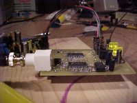
Here's a contest: spot the missing wire in the PCB layout.
-jwb
Here's a contest: spot the missing wire in the PCB layout.
-jwb
About your transformer.........
If I read your drawing correctly, you are connecting it directly to the RXP and RXN pins of that Crystal receiver?
Jocko
If I read your drawing correctly, you are connecting it directly to the RXP and RXN pins of that Crystal receiver?
Jocko
Re: About your transformer.........
Tacky, isn't it? But I tried it out with these parts and saw no trouble. The pattern was clean with the trafo coupled directly to the 8420. I measured it on tx and rx side of cable with my full battery of space-aged instrumentation*.
-jwb
* A low-dollar Tek 100MHz digital scope + math module.
Jocko Homo said:If I read your drawing correctly, you are connecting it directly to the RXP and RXN pins of that Crystal receiver?
Tacky, isn't it? But I tried it out with these parts and saw no trouble. The pattern was clean with the trafo coupled directly to the 8420. I measured it on tx and rx side of cable with my full battery of space-aged instrumentation*.
-jwb
* A low-dollar Tek 100MHz digital scope + math module.
I know the layout is easier, but.....
Those inputs are Schmitt trigger types.......saturated logic.......very bad for reflections. It will sound and measure much better with some type of buffer in between.
I built a D/A convertor prototype once in one night's work. Spent the next 6 months getting all the reflections out of the circuit.
Jocko
I'm quite pleased to report that this unit works as drawn. I completed my prototype assembly tonight. It starts and runs perfectly well. There are startup and shutdown transients of approximately 3Vp-p at 10Hz, so be careful when testing.
The mistake I made in the layout, which nobody took my challenge of finding, is a missing trace between the LEDs in the current source for the line driver on the left channel. I had to bridge that with a bit of wire.
Also, I mistakenly rotated the two pull-down resistors on the right of the CS8420when assembling, and it took some time to find that problem. Be careful, and next time I'll draw them assymetrically.
The unit sounds fine through my impossibly mediocre bench test speaker. I'll be able to report more after I put the chassis together and bring this DAC into my listening room.


Did the pcb have split groundplane? Have you made any tests with RF-emission. Can you listen to radio/TV near the DAC?

Unused pins and mode pins...
Hi
I'm putting together a similar circuit(but with AD1853), but am new to the digital side and had a question on your layout. On the Cs8420 you have pull down resistors on the unused pins. Is this the best way to deal with them or can they be left floating, or just grounded?
Also the spec sheet shows 3 of the HW mode1 select pins direct to ground, and you have pulldowns on those also (DFC0 DFC1 S/AES) at your original 4.75K value this is pretty close to gnd, but with the spec'ed 47.5k they're a bit off the ground?
Is it better for noise to be using the pull downs, or just for consistency. I'm just trying to learn the ropes.
Thanks for the circuit and layout, it has definitely jump started my own project! I hoping for a reasonably good DAC w/ which I can play with clocks, IV stages etc. All that will be off board.(but close by)
-Pete Kunz
pjkunz said:Unused pins and mode pins...
Hi
I'm putting together a similar circuit(but with AD1853), but am new to the digital side and had a question on your layout. On the Cs8420 you have pull down resistors on the unused pins. Is this the best way to deal with them or can they be left floating, or just grounded?
Actually I have pull-downs on the pins because that is how the CS8420 configures itself. In hardware mode, the 8420 needs pull-up/down on each pin to set the options. Check the datasheets for the hardware mode options.
Also the spec sheet shows 3 of the HW mode1 select pins direct to ground, and you have pulldowns on those also (DFC0 DFC1 S/AES) at your original 4.75K value this is pretty close to gnd, but with the spec'ed 47.5k they're a bit off the ground?
I wanted the 4.7K to ground because, as you point out, it improved the logic margin. But, this makes the chip sink a lot of current per pin, so I reverted to 47K. I don't have any problems.
-jwb
Hi, thanks for the reply,
I understand the pull/up/downs for the startup pin settings, but was curious about the best way to deal with the pins that are completely unused such as TXN, TXP, etc. and also have no startup function in HWM1. You have pulldowns on all of them and I was just curious...
I understand the pull/up/downs for the startup pin settings, but was curious about the best way to deal with the pins that are completely unused such as TXN, TXP, etc. and also have no startup function in HWM1. You have pulldowns on all of them and I was just curious...
Well okay, I forgot about TXP and TXN. I pull them to ground to keep them from picking up noise.
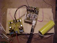
Oops. I just got the transformers in from Scientific Conversions. They are bigger than the pads I drew for them. Another board bug. Luckily my CD player has a transformer-coupled output. With all these bugs piling up, I should me a second revision.
You could get those boards for cheaper from olimex. And they would also have soldermask and silkscreen. I used them for a fine pitch smd design I did. They are $26 for whatever you can fit in 100x160mm. I got five different boards in mine and they didn't complain. They even take eagle files directly. http://www.olimex.com The DAC looks nice.
Darrell Harmon
Darrell Harmon
If you need to order multiple boards for the second revision, I might go in with you. I was thinking about building a converter using this chip for a while now, but never got around to coming up with a good schematic. I'm interested in it as a way to take the S/PDIF output of my MP3 player and feed it to a better DAC, to drive headphones, which presents its own post-DAC amplification issues as well. However, your circuit is a good start for the DAC portion.
Mike
Mike
jwb said:Oops. I just got the transformers in from Scientific Conversions. They are bigger than the pads I drew for them. Another board bug. Luckily my CD player has a transformer-coupled output. With all these bugs piling up, I should me a second revision.
- Status
- Not open for further replies.
- Home
- Source & Line
- Digital Source
- Cheap 24/96 DAC with CS43122