A continuation of my previous thread, Rolecor RTA-650 receiver - revisited. But will bypass those details. I am failing to solve a problem or discoveed another, and I am hoping for additional, insightful advice.
Where I am at now is BD139 & BD140 driver transistors are installed. They are in place of KSA2690 & KSA1220 which themselves replaced original 2SC497 & 2SA497 as one of the latter was faulty.
Newly received output devices are in place as well, MJ21194.
After each transistor installation, I powered the receiver up with a DBT and each time, the bulb settled to a dull glow. Once all were installed, I tried listening to the receiver but still have a dead channel - the right one.
Before installing the BD139 & BD140 pairs, I was getting 53 Volts at each leg of the transistors preceeding them. And I am still getting that voltage now.
Looking to an "upstream" component, I checked a TO18 transistor in the affected channel and it reads as bad. It's counterpart in the other channel does not display the same fault.
The number is C727 - presumably 2SC727.
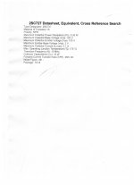
So far, my searching has not hit on any situation involving that transistor. I did find a data sheet (attached) but when entering specs on Digi Key's part finder, which is just guessing on my part, no results resemble what I think I'm looking for.
Since a C727 is NPN, I don't suppose BD139's that I ordered extras of would do?
Where I am at now is BD139 & BD140 driver transistors are installed. They are in place of KSA2690 & KSA1220 which themselves replaced original 2SC497 & 2SA497 as one of the latter was faulty.
Newly received output devices are in place as well, MJ21194.
After each transistor installation, I powered the receiver up with a DBT and each time, the bulb settled to a dull glow. Once all were installed, I tried listening to the receiver but still have a dead channel - the right one.
Before installing the BD139 & BD140 pairs, I was getting 53 Volts at each leg of the transistors preceeding them. And I am still getting that voltage now.
Looking to an "upstream" component, I checked a TO18 transistor in the affected channel and it reads as bad. It's counterpart in the other channel does not display the same fault.
The number is C727 - presumably 2SC727.
So far, my searching has not hit on any situation involving that transistor. I did find a data sheet (attached) but when entering specs on Digi Key's part finder, which is just guessing on my part, no results resemble what I think I'm looking for.
Since a C727 is NPN, I don't suppose BD139's that I ordered extras of would do?
Attachments
Last edited:
Erm....its only a 350 mW, small signal transistor so any TO92 style amplifier with a Vceo > 75V will probably do. 2N5551 is cheap, common and also a good candidate for voltage amplifier duty. The pinout is different to Japanese transistors so you need to identify the correct leads by looking up the pinout. Note that 2N5551C is an oddball spec. in Japanese style, with the collector in the centre.
To check physical formats and leads, just type 2Nxxxx or whatever you need into your browser, followed by "pinout" and press enter.
Alternatively, you could use the KSC2690A type which is somewhat similar and you already have but it may be a tight fit. As before, check the pinout and also the fit of the leads in the pcb.
Thanks for that tip! If a KSC2690A will fill the bill, that's what I shall use.
Those were what went in to replace original "flying saucer" transistors and I managed to safely enlarge the holes Or I whittled down the legs, one or the other.
I plan to check voltages at 2SC727 to determine if it too has 53 volts al around.
Even though a DBT reacted properly, can I assume that the BD139 and/or BD140 are destroyed from 53 volts being present at Emitter, Base & Collector?
You can read the datasheets which show BD139/140 Vceo max. is 80V. That should be fine, assuming your line voltage is at the rated 110V so that the DC supply to the amplifier remains within safe limits. We don't really know that the measured 53V (presumably with respect to chassis ground) at the 2SC727 collector is correct anyway. Check and compare with the collector voltages of the output transistors, which should be similar for one transistor and half that for the other. In any case, failures are seldom due to mains voltage variations provided parts ratings are chosen to be adequate and other parameters are suitable for the duty.
If the output stage is toast or perhaps just overloaded, the voltage amplifier (2SC727) will then be attempting to drive a virtual short and that overload likely causes its failure too. All this happens in a flash so there is little point in trying to investigate or prove events only milliseconds apart if you still wind up with the same chain of failed semis, perhaps because you haven't cleared all the likely collateral damage after each event nor replaced any bad electrolytic caps.
A DBT works by severely limiting supply current to a level that really only maintains the standby or idling current drawn by the device under test. Most articles written about DBTs are for tube amps which have a high idling current due to their heaters but semiconductor amps usually have low idling current and the older, smaller and simpler types generally draw the least. That means you need to choose your lightbulb rating carefully and a small 45W rating would be enough for a small amplifier or receiver, assuming you turn the receiver part off and so are any incandescent lamps inside. You can use a 60W bulb at a pinch and some repairers use even higher when they want the amp. to produce a little audio too but the safety part then becomes more a risk level decision you make. With experience, you might do that, otherwise don't. You may be using halogen lamps which also work but the available ratings are often quite different to the old type so you may have to compromise there.
You may wonder why an old amplifier suddenly starts to blow semis yet nothing had changed in its use. I came across a lot of them though, typically re-purposed by folk who were now accustomed to newer, fully protected gear. The general problem with old amps though, is their old deteriorated capacitors and dodgy protection systems that no longer work properly. They may limp along with weak performance but that soon turns to expensive failures without a proper service including a full recap.
Just checked Collector voltges on the ouputs as suggested. There are two devices per channel and the affected channel has 53 collector volts on each.
The unaffected side has 18 volts on one and approximately 53 volts on the other.
One of the TO3's with 53 collector volts also has 53 volts at the emitter and base. Not so with the other TO3 in that channel.
I must give this a rest for a day or two. It's eating up too much of my thought processes.
So despite there being 53 volts where there should be less does not necessarily mean that device is damaged? I would hate that to be so for the MJ21194 outputs since they were $10 plus per piece.
A couple of days later and still flummoxed.
Two things done today, replaced the bad channel's 2SC727 with a C2609 as suggested plus, following a tip from someone, replaced a thermistor that I thought was a diode with (2) IN4148's in series.
None the less, I am still reading 53 volts in places where readings at the same spots in the opposite channel are 18 volts.
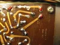
As example, the pads marked B1 & b1. There are 53 volts at pad B1 as there is at the same spot on the "good" channel. But b1 also has 53 volts whereas b1 at the other board reads 18 volts.
The affected board is not big and not densely populated so I am contemplating "shotgunning" it.
Two things done today, replaced the bad channel's 2SC727 with a C2609 as suggested plus, following a tip from someone, replaced a thermistor that I thought was a diode with (2) IN4148's in series.
None the less, I am still reading 53 volts in places where readings at the same spots in the opposite channel are 18 volts.
As example, the pads marked B1 & b1. There are 53 volts at pad B1 as there is at the same spot on the "good" channel. But b1 also has 53 volts whereas b1 at the other board reads 18 volts.
The affected board is not big and not densely populated so I am contemplating "shotgunning" it.
Attachments
With the upper (see earlier link) power transistor which you say has 53V on the collector and effectively the same voltage on the emitter, it means they must be shorted. Recheck by measuring directly between collector and emitter (watch you don't slip) If the voltage is very small, it's likely toast. At this point, we need the real schematic to predict what the key voltages should be but without it or at least good, clear pictures, that requires long experience or some reverse-engineering skill which doesn't come easy to everyone.
A check shows most models in that era had split power supplies of about +/-29V wrt ground and had a fuse in each speaker output . Some small models only had a single supply of up to the total voltage of the split ones but would also have a big capacitor of 1,000 uF or more in lieu of each fuse. Perhaps you can identify such a caps. in series with the output, as distinct from those in the power supply and associated with the rectifier diodes.
The fact that you measure 53V wrt ground is confusing. It doesn't seem to equate to the size of the original output transistors so we need more information to be certain of anything.
May I suggest you don't try the shotgun approach to repairs where semis are involved because it means substituting to replace them which, as you find, can be expensive but that's not all - it typically creates a worse situation that is hard to go back from when these also fail because they are not really equivalent parts.
It's also likely that the amplifier then won't work properly because of the combined effect of the differences between the original and substitute semis. Rescuing that situation will just become progressively harder if you can only choose from the dwindling number of similar and current production thru-hole parts available from local distributors. Best is to keep the original semis if you can but this comes down to awareness, appropriate measurements and experience of what parts are at high risk and what doesn't make much difference. Tougher transistors may seem a logical solution to failures but it also means wider collateral damage when they too, expire.
Use your DMM to measure for shorts between collector and emitter of all the transistors in the sick power amplifier and also measure Vbe (shorthand for the small voltage between base and emitter). It should be in the region of a diode voltage drop - about 0.65V either positive or negative, depending on whether it's NPN or PNP. You check all transistors because you don't know whether the output transistor failure also caused more failures going back to the input, as it seems occurred with the 2SC727. It's not unusual to do more damage yourself when measuring in tight spots - use at least one hook probe or clip leads unless confident that you will never slip up.
Unfortunately, I suspect the MJ21194 is now toast too but there could be other problems that only make it seem that way. Otherwise, from the bitter experience of taking on repairs unwisely, I never buy or accept stuff, working or not, that I can't get at least the schematics for. They are priority support so download what you can if its virtually free. It can then be easily forwarded or posted for others who may be able to make better suggestions for you to try in your own time.
To make sure my transistor checking was done without "outside influence" I pulled all of them and tested all with a DMM in diode mode. With the exception of MJ21194's all checked out OK and went back into place. This included all TO92's, the BD139/BD140 pair plus the KSC2690A.
You were correct in that the MJ21194's were damaged....all 4 of them and are currently off the receiver.
I cannot explain why that is other than my having them all out once or twice, and perhaps installing those that were in the working channel into the affected "bad" channel.
Or perhaps accidentally shorting speaker outputs? The receiver is capacitor coupled and as far as I am aware, has no speaker protection.
With all four output transistors removed, what I observed is that the 53 volts is not present at places on the "bad" board where it was before. In spots where the "good" channel was reading 18 volts (and the bad 53 volts), I now see about 12 volts at the corresponding points of the"bad" board. Not 18 volts but down a lot from 53 volts.
It crossed my mind that this 18 volt vs 12 volt difference might be because the "good" board still has an 2SC727 wheras the "bad" board (with 12 volts) has the KSC2690. I am considering replacing that other 2SC727 with a KSC2690 to see if the 18 volts on that side also drops to 12 volts.
I observed something else interesting, at least to me.
With all outputs removed, I plugged in some headphones and got audio, equal on both channels.
And with the outputs removed, I measured voltages to all of the collector connections.
One of the two output device sockets on each channel has 53 volts at it's collector point. The 2nd output device socket on each channel were unequal at 18 volts at the "good channel" and about 11 volts at the bad channel - where there had been 53 volts.
Might it be, the absence of output transistors caused this voltage "correction"? Or in other words, did a faulty one cause the overall voltage increase to 53 volts?
I did remove and replace all the transistors on the board, as previously mentioned, but replaced none.
In your opinion, if invested in another quad of MJ21194's would they be at risk when installed?
FWIW, rail voltage in this unit is 53 volts. A lot, I thought, for something with minimal output watts. The original single filter cap was rated at 63 volts as is it's replacement.
EDIT: Another thought occurred. Is it possible a collector to chassis short is created when the output transistors are secured into place?
Last edited:
Too late for an edit.
4th sentence up from the bottom should read:
I did remove and reinstall all the transistors on the board, as previously mentioned, but replaced none.
4th sentence up from the bottom should read:
I did remove and reinstall all the transistors on the board, as previously mentioned, but replaced none.
And I made a gross error when testing the MJ21194 outputs
Like an ***, I had the B & E pins reversed. Re-checking those output devices again just now turned out positive results in that all four MJ21194's are OK.
My next move will be re-installing them, bring up voltage to the receiver with a variac and monitor what the collector voltages are. If the pattern of the "good" channel is duplicated, there will only be 53 volts at the collector of one output transistor of the "bad" channel, not both.
Success at least for now
After becomming aware of my ineptness in determining base from emitter and realizing the output transistors were good after all, I reinstalled them.
Whether it was adviseable or not, I brought up the receiver's power with a variac. This time, the output transistor's collector voltages were different. The "bad channel" was 53 volts on one and about 11 volts on the other.
Unsure if it would make a difference, I opted to replce the 2SC727 on the "good board" with a KSC2690 to duplicate the "bad board".
This did nothing to equalize collector voltages, they stayed at 18 volts for left side and 11 volts for right.
I did however descover that rotating the much larger of the two variable resistors on the board adjusted this collector voltage. Unsure of what it should be, I upped the 12 volts of the right (bad) board to 18 volts to mimic the left (good) board.
I cannot appreciate the exact reason why, but the 53 volt anomaly is gone now and the receiver seems to work well. At least as near as I can tell it's working well.
Now I must attampt to ducument the changes I made to the transistors and replacement resistors.
Hoping it's not premature, but thanks Ian et al for the patient assistance.
Last edited:
Re collector short: Yes, as the collector is also connected to the transistor case, anything metallic like metal fragments can short this to the heatsink or chassis, even puncture the insulating washer (silicone rubber or mica/grease). If the clearance holes are tight enough, even the leads and mounting bolts can short to the chassis if they aren't insulated with suitable sleeving or bushes. Then always use your meter to prove there is no continuity from ground to any part of the transistor after fitting but before soldering. Note: the lower power output transistor emitter will actually be grounded since it is at 0V.
As both the replacement semis have now failed, you have changed something else that was previously OK. If you continue to try a series of changes before testing each one properly, the situation can only get worse. Sorry, but that's simply logical deduction.
This is an old style amplifier known as a "Quasi-complementary" design. i.e. the same NPN transistor is operated as a complement to the other but they are actually the same type. (hence "quasi") Not only that, as you see, there is only a single voltage rail and the output of the amplifier should ideally be at half that voltage. So with no load or signal, you should be seeing 53 volts at the top transistor collector but only approximately 26.5V at its emitter and also at the collector of the lower transistor. The emitter of the lower transistor is at approx. 0V.
In modern designs, true complementary transistors are now used and generally, two rail voltages of +/- 26.5V would also be used to power it in a true complementary circuit. This will have circuitry that is mirrored on +/- sides of the output point and so will the DC voltages on either + or - supply side. The sum of those two, split supply voltages is the same 53V as used in the quasi-comp. design, so nothing much has changed between the two circuit arrangements, other than you now have to isolate that +26.5V DC with a capacitor, to protect the speaker voice-coil from burning out with the applied DC.
BTW, as you now have repeat failures, something is obviously still wrong, so just replacing those semis will end the same way. Stop, look at what you have already done. Identify and test the voltages of all solder points of the power and driver transistors and the voltage amplifier (now BD139) without the output transistors in place. Post them here, alongside those of the good channel:
Here is is a clear description of a quasi-comp. amplifier design; how it's different and other typical design shortcuts that were commonly used together with it in earlier times. There are plenty more good learning articles in the archive of Radio-Electronics magazine which will be worth your time to study: Quasi Complementary Transistor Output >> Electronics Notes
edit: sorry, our posts crossed so much of this may not now apply.
- Home
- Amplifiers
- Solid State
- Chapter 2 - Rolecor RTA-650 receiver - revisited....a (2S)C727 replacement?