In post #4 under
https://www.diyaudio.com/community/threads/compensation-capacitor-cdom.105453/
I read this:
The Cdom is the easy and very effective solution that virtually guarantees stable operation of a three stage "LIN" topology.
But the downside is reputedly poor sound quality.
Try the non-inverting input for improved sound quality.
And use a very low capacitance transistor for VAS to reduce the current that gets sucked out of the LTP.
D. Self does not mentioned various alternatives - only the usual circuit topology for Cdom from collector to base of VAS transistor is described.
The only way I know to avoid Cdom at whole is the use of only one voltage gain stage - this means mostly a folded cascode (like realized in the AVM mono blocks and in the internal circuit of AD817 and AD797.
But this means in discrete versions less open loop gain.
Some other approaches in power amps with two gain stages (i. e. LTP+VAS) is the attempt, to use the inverted input for Cdom (often with serial resistor) - check out the schematics in attachment three and four.
But I want to know exakt design rules for compensation steps at whole (without typical Cdom to avoid unwanted oscillation).
Thanks for any advice.
P.S.:
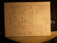
This desire arose after I receive a Horch 3.0s power amplifier that have unwanted oscillation - check out schematic with two voltage gain stages in the first attachment.
Here are to find some capacitors for compensation - partly at unusual places.
But at the usual place for Cdom in the VAS stage there are no capacitor to find (also not at the input for low pass function).
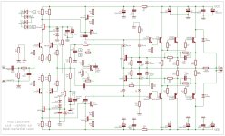
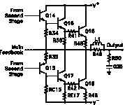
Most other amplifiers with similar topologies use there capacitors - go to the second attachment for an example (schematic of Leach amp).
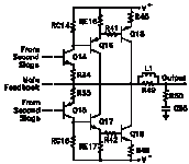
Maybe an important fact to determine this exactly is the kind of output stage configuration (darlington emitter follower or CFP power output stage - go to the attachment five and six) so as the sequence of the serial inductor and the Boucherot cell (Zobel network) at the speaker output - go to the last attachment (Zobel network sometimes behind the inductor, sometimes in front of the inductor - i. e. just on the power amp output, which seems more plausible to me - go to
https://www.diyaudio.com/community/...an-inductor-on-my-class-ab-amp-output.346796/
and read from post #7)
https://www.diyaudio.com/community/threads/compensation-capacitor-cdom.105453/
I read this:
The Cdom is the easy and very effective solution that virtually guarantees stable operation of a three stage "LIN" topology.
But the downside is reputedly poor sound quality.
Try the non-inverting input for improved sound quality.
And use a very low capacitance transistor for VAS to reduce the current that gets sucked out of the LTP.
D. Self does not mentioned various alternatives - only the usual circuit topology for Cdom from collector to base of VAS transistor is described.
The only way I know to avoid Cdom at whole is the use of only one voltage gain stage - this means mostly a folded cascode (like realized in the AVM mono blocks and in the internal circuit of AD817 and AD797.
But this means in discrete versions less open loop gain.
Some other approaches in power amps with two gain stages (i. e. LTP+VAS) is the attempt, to use the inverted input for Cdom (often with serial resistor) - check out the schematics in attachment three and four.
But I want to know exakt design rules for compensation steps at whole (without typical Cdom to avoid unwanted oscillation).
Thanks for any advice.
P.S.:
This desire arose after I receive a Horch 3.0s power amplifier that have unwanted oscillation - check out schematic with two voltage gain stages in the first attachment.
Here are to find some capacitors for compensation - partly at unusual places.
But at the usual place for Cdom in the VAS stage there are no capacitor to find (also not at the input for low pass function).
Most other amplifiers with similar topologies use there capacitors - go to the second attachment for an example (schematic of Leach amp).
Maybe an important fact to determine this exactly is the kind of output stage configuration (darlington emitter follower or CFP power output stage - go to the attachment five and six) so as the sequence of the serial inductor and the Boucherot cell (Zobel network) at the speaker output - go to the last attachment (Zobel network sometimes behind the inductor, sometimes in front of the inductor - i. e. just on the power amp output, which seems more plausible to me - go to
https://www.diyaudio.com/community/...an-inductor-on-my-class-ab-amp-output.346796/
and read from post #7)
Attachments
-
 Horch 3.0s schematic.jpg285.3 KB · Views: 175
 -
 LEACH Amp Schematic.jpg117.6 KB · Views: 154
 -
 Crimson Power Amplifier Issue VII schematic.jpg308.5 KB · Views: 169
 -
 JLH 80w mosfet power amplifier.jpg56.6 KB · Views: 152
 -
 outstage3.gif4.2 KB · Views: 142
 -
 outstage2.gif4.3 KB · Views: 146
 -
Output-L_1.pdf866.6 KB · Views: 64
Last edited:
Not true at all, he explains several alternative compensation schemes, such as output-inclusive and two-pole, in "Audo power amplifier design" he has a whole chapter on compensation schemes. Worth a read.D. Self does not mentioned various alternatives - only the usual circuit topology for Cdom from collector to base of VAS transistor is described.
The reason for low-capacitance VAS transistor is better linearity, not stability. Stability requirements are mainly controlled by the inherent low-pass poles in the output section.
Distortion at 1kHz and below is usually not limited by which compensation scheme is used, but up at 5kHz--10kHz region more elaborate compensation can benefit the distortion performance by maximizing open-loop gain.
I got 108 dB of open loop gain at 20 kHz in a single-stage amplifier with discrete transistors. This can also be solved.The only way I know to avoid Cdom at whole is the use of only one voltage gain stage - this means mostly a folded cascode (like realized in the AVM mono blocks and in the internal circuit of AD817 and AD797.
But this means in discrete versions less open loop gain.
Your Leach amp circuit is posted with connection error T16 T17check out the schematics in attachment ....Most other amplifiers with similar topologies use there capacitors - go to the second attachment for an example (schematic of Leach amp).
maximum linearity and maximum gain of the first input stage - by solving this problem using zero and first order circuits, you yourself will understand the principles of compensation.But I want to know exakt design rules for compensation steps at whole (without typical Cdom to avoid unwanted oscillation).
Thanks for any advice.
With multi-pole correction, not everything is so simple; in blind tests, amplifiers with such correction were inferior in terms of sound preference despite low measured distortion, except for those where the depth of negative feedback at a frequency of 20 kHz exceeded the threshold of 90 dB
It is three-stage, which is difficult to coordinate with compensation circuits in the form of shunts.This desire arose after I receive a Horch 3.0s power amplifier that have unwanted oscillation - check out schematic with two voltage gain stages in the first attachment.
Last edited:
This is what the gain of an open loop looks like for a single-stage amplifier, and this is not a composite.
